
10M16SAU169I7G Datasheet, Specifications & Application Guide – Altera MAX 10 FPGA
The 10M16SAU169I7G is a non-volatile FPGA from the Altera (Intel) MAX 10 family. Built on a 55 nm process with 16,000 logic elements, integrated dual ADC, and instant-on flash configuration, it targets industrial control, IoT edge processing, and mixed-signal embedded systems. This guide covers its full datasheet parameters, pinout, block diagram, application circuits, and design tips.

Table of Contents
- 1. 10M16SAU169I7G Overview & Part Number Decoding
- 2. Key Specifications & Electrical Parameters
- 3. Block Diagram & Internal Architecture
- 4. Pinout, Package & Footprint (U169 UBGA)
- 5. Application Circuit & Design Guidelines
- 6. FAQ – 10M16SAU169I7G
1. 10M16SAU169I7G Overview & Part Number Decoding
The 10M16SAU169I7G belongs to the Intel (Altera) MAX 10 FPGA family, the industry's first single-chip non-volatile FPGA with integrated analog capabilities. Unlike traditional FPGAs that require external configuration flash, MAX 10 devices store their configuration internally and power up instantly—ideal for applications where boot time matters.
Part Number Breakdown
| Segment | Value | Meaning |
|---|---|---|
| 10M16 | MAX 10, 16K LEs | Device family and density |
| S | Single supply | Single 3.3 V power supply operation |
| A | Analog | Integrated ADC enabled |
| U169 | 169-ball UBGA | Ultra-thin Ball Grid Array, 11 × 11 mm |
| I | Industrial | −40 °C to +100 °C operating range |
| 7 | Speed grade 7 | Fastest speed grade available |
2. Key Specifications & Electrical Parameters
| Parameter | Value |
|---|---|
| Logic Elements (LEs) | 16,000 |
| Logic Array Blocks (LABs) | 1,000 |
| Embedded Memory (M9K) | 549 Kbit |
| User Flash Memory (UFM) | 2,304 Kbit |
| 18 × 18 Multipliers | 45 |
| PLLs | 4 |
| Maximum User I/O (U169 pkg) | 130 |
| LVDS Pairs | Up to 22 |
| Analog-to-Digital Converter | Dual 12-bit, 1 MSPS ADC |
| ADC Channels | Up to 18 analog inputs |
| Core Voltage | 1.2 V |
| I/O Voltage | 1.0 V to 3.3 V |
| I/O Standards | LVTTL, LVCMOS, SSTL, HSTL, LVDS, TMDS |
| External Memory Interface | DDR2, DDR3, LPDDR2, SRAM |
| Configuration | Internal flash (instant-on), dual boot image support |
| Package | 169-ball UBGA (11 × 11 mm, 0.8 mm pitch) |
| Temperature Range | −40 °C to +100 °C (Industrial) |
| Speed Grade | 7 (fastest) |
| Process Node | 55 nm |
| Bitstream Security | AES-128 encryption supported |
3. Block Diagram & Internal Architecture
The MAX 10 architecture integrates logic, memory, DSP, ADC, and flash configuration on a single die. Below is the functional block diagram showing the key subsystems of the 10M16SAU169I7G:
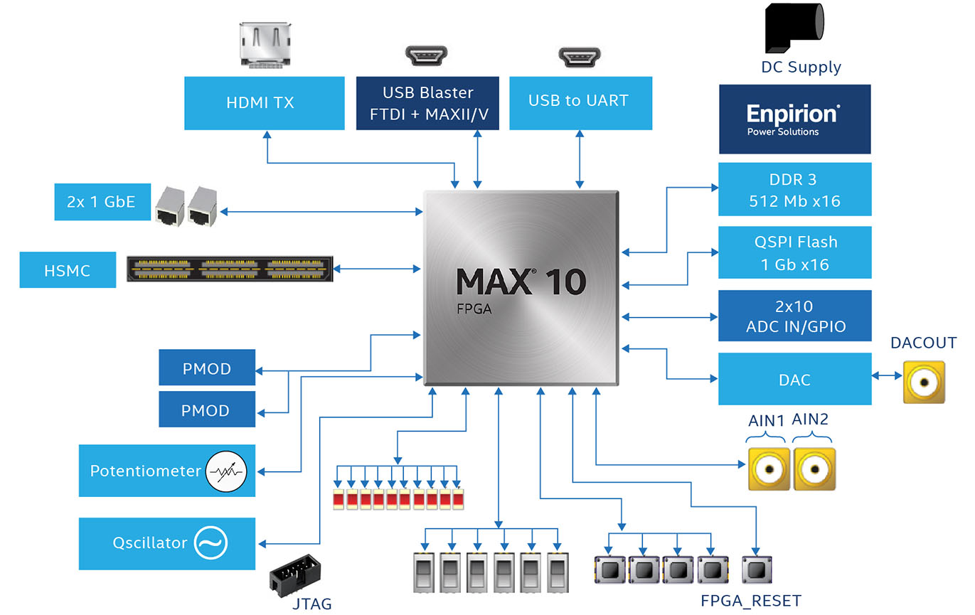
Key architectural highlights:
- Logic Array: 1,000 LABs each containing 16 adaptive logic modules (ALMs) with 4-input LUTs and dedicated carry chains.
- Embedded Memory: M9K blocks (9 Kbit each) configurable as single-port RAM, dual-port RAM, ROM, or FIFO.
- DSP Blocks: 18 × 18 multipliers for signal processing, filter, and math operations.
- Dual ADC: Two 12-bit SAR ADCs with up to 1 MSPS sample rate, enabling direct analog sensor interfacing.
- Configuration Flash Memory (CFM): Stores up to two configuration images for fail-safe remote update.
- User Flash Memory (UFM): 2,304 Kbit of on-chip flash for storing coefficients, calibration data, or small program code.
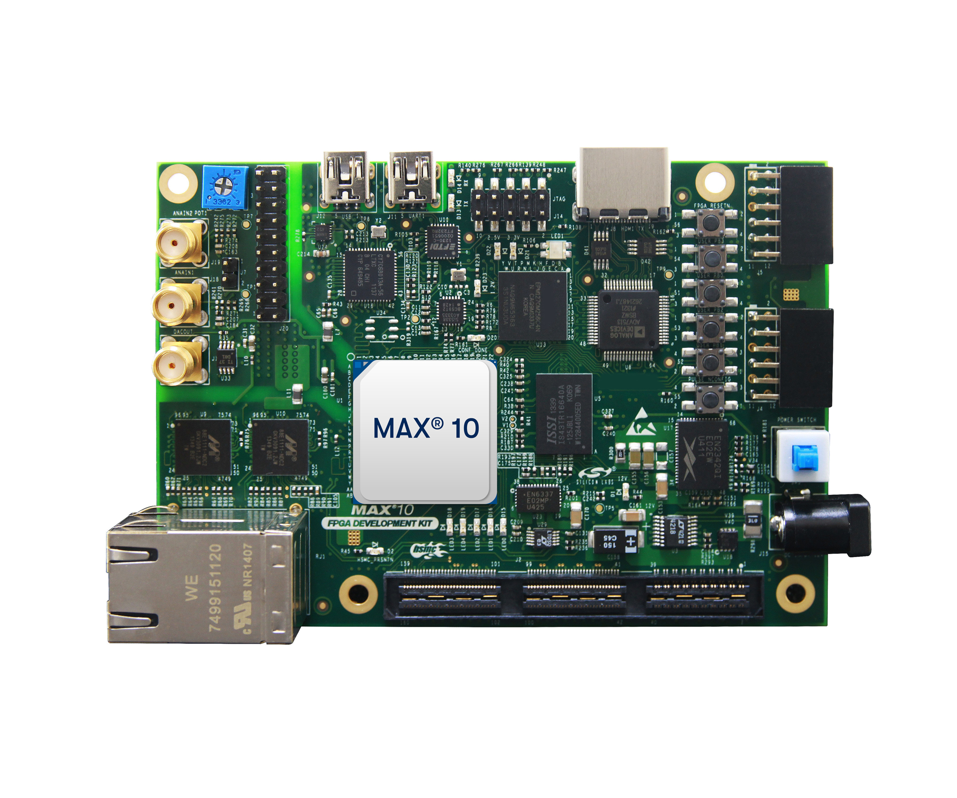
4. Pinout, Package & Footprint (U169 UBGA)
The 10M16SAU169I7G is housed in a 169-ball UBGA package with a compact 11 × 11 mm body and 0.8 mm ball pitch. The package provides 130 user I/O pins across 8 I/O banks, supporting a wide range of voltage levels and differential signaling standards.
Pin Categories
- User I/O: 130 general-purpose I/O pins configurable per bank voltage
- Dedicated Clock Inputs: 4 dedicated clock input pins for low-jitter clock distribution
- JTAG: TDI, TDO, TMS, TCK for programming and debug via IEEE 1149.1
- ADC Inputs: Dedicated analog input pins routed to the dual 12-bit ADC
- Power/Ground: VCC (1.2 V core), VCCIO (per-bank I/O), VCCA (analog PLL), GND
PCB Design Tips: Use a minimum 4-layer stackup. Place 100 nF decoupling capacitors close to each VCC/VCCIO ball. Route LVDS pairs with controlled impedance (100 Ω differential). Keep analog input traces short and shielded from digital switching noise.
5. Application Circuit & Design Guidelines
The 10M16SAU169I7G is a versatile FPGA suited for a variety of embedded and industrial applications. The integrated ADC and instant-on capability make it particularly attractive for mixed-signal designs that require fast startup and analog sensing.
Typical Application Areas
- Industrial Control & Motor Drives: Real-time PWM generation, encoder interfaces, and sensor fusion with on-chip ADC.
- IoT Edge Gateway: Protocol bridging (SPI/I2C/UART to Ethernet), local data preprocessing, and over-the-air firmware update via dual-boot flash.
- Video & Image Pre-processing: Bayer demosaicing, color space conversion, and frame buffering for camera modules.
- Medical Instrumentation: Multi-channel ADC data acquisition, digital filtering, and low-latency control loops.
- Test & Measurement: Custom protocol analyzers, pattern generators, and data logging with UFM storage.
Power Supply Recommendations
| Rail | Voltage | Purpose |
|---|---|---|
| VCC | 1.2 V | FPGA core logic |
| VCCIO | 1.0 – 3.3 V | I/O bank supply (per bank) |
| VCCA | 2.5 V | PLL analog supply |
| VCCD_PLL | 1.2 V | PLL digital supply |
| VCC_ADC | 2.5 V | ADC supply |
For single-supply operation (S variant), the device can derive all internal supplies from a single 3.3 V input using the internal voltage regulators, simplifying board design.
Video Tutorial
Watch this tutorial on getting started with MAX 10 FPGA development using Quartus Prime:
6. FAQ – 10M16SAU169I7G
Q1: What is the difference between 10M16SAU169I7G and 10M16SAU169C8G?
The "I7" suffix indicates industrial temperature range (−40 °C to +100 °C) with speed grade 7 (fastest), while "C8" denotes commercial temperature (0 °C to +85 °C) with speed grade 8 (slower). Choose the I7G variant for harsh-environment or wide-temperature applications.
Q2: Does the 10M16SAU169I7G require an external configuration flash?
No. MAX 10 devices feature internal configuration flash memory (CFM), enabling instant-on operation without any external configuration PROM or flash. The device supports dual-image storage for fail-safe remote updates.
Q3: How many ADC channels are available?
The 10M16SAU169I7G integrates a dual 12-bit ADC with up to 18 analog input channels and a maximum sample rate of 1 MSPS. The ADC can be used for temperature sensing, voltage monitoring, or external analog signal acquisition.
Q4: What software tools are needed to program the 10M16SAU169I7G?
Use Quartus Prime Lite Edition (free) from Intel/Altera for synthesis, place-and-route, timing analysis, and JTAG programming. The Nios II soft processor and Platform Designer (formerly Qsys) are also supported for embedded system designs.
Q5: Can the 10M16SAU169I7G interface with DDR3 memory?
Yes. The MAX 10 family supports DDR3, DDR2, LPDDR2, and SRAM external memory interfaces. Use the External Memory Interface IP core in Quartus to configure the memory controller with proper timing calibration.
Q6: What development boards support the MAX 10 16K LE device?
Popular options include the Terasic DE10-Lite (10M50 variant), the Arrow MAX1000, and the Altera MAX 10 FPGA Development Kit. These boards provide USB-Blaster programming, expansion headers, and onboard peripherals for rapid prototyping.


