
Overview of the 10M16SAU169I7G
The 10M16SAU169I7G is a non-volatile FPGA from the Altera (now Intel) MAX 10 family, fabricated on a mature 55 nm process node. It delivers 16,000 logic elements, an integrated dual-channel 12-bit ADC, and on-chip user flash memory—all in a compact 169-ball UBGA package. Because MAX 10 stores its configuration in internal flash, the device powers up instantly without requiring an external configuration PROM, dramatically simplifying board design and reducing BOM cost.
The part number decodes as follows: 10M16 = MAX 10 with 16K logic elements, S = single-supply operation, A = analog block (ADC enabled), U169 = 169-ball UBGA package, I = industrial temperature range (−40 °C to +100 °C), 7 = speed grade 7.
Designers choose this device for industrial control, motor drives, sensor-hub aggregation, and cost-sensitive IoT gateways where instant-on behavior, integrated analog, and a small footprint are critical. Browse more FPGA options at wwdparts.com/collections/fpga.
Key Specifications & Parameters
| Parameter | Value |
|---|---|
| Manufacturer | Altera (Intel) |
| Family | MAX 10 |
| Part Number | 10M16SAU169I7G |
| Logic Elements (LEs) | 16,000 |
| Embedded Memory (M9K) | 549 Kb |
| User Flash Memory (UFM) | 2,304 Kb |
| 18 × 18 Multipliers | 45 |
| PLLs | 4 |
| Global Clock Networks | 20 |
| Maximum User I/O | 130 (U169 package) |
| ADC | Dual 12-bit, 1 MSPS |
| Package | 169-ball UBGA (11 × 11 mm) |
| Process Technology | 55 nm |
| Core Voltage | 1.2 V (single-supply: 3.3 V input) |
| Operating Temperature | −40 °C to +100 °C (Industrial) |
| Speed Grade | 7 |
| External Memory Interface | DDR2, DDR3, LPDDR2, SRAM |
| Configuration | Internal flash (instant-on, no external PROM) |
| Bitstream Security | AES-128 encryption |
Need a different variant? Explore the full MAX 10 FPGA lineup at wwdparts.com.
Block Diagram & Architecture
The MAX 10 architecture integrates logic elements, M9K embedded-memory blocks, DSP multiplier blocks, PLLs, a dual-channel ADC, and user flash memory into a single monolithic die. The diagram below illustrates how these functional blocks interconnect through the device's row-and-column routing fabric.
Key architectural highlights include single-supply operation (internal voltage regulators derive the 1.2 V core from a 3.3 V input), dual configuration-image support for safe remote firmware updates, and a hard ADC block that eliminates the need for an external ADC chip in mixed-signal designs.
Pinout, Package & Footprint
The 10M16SAU169I7G ships in a 169-ball UBGA package measuring 11 × 11 mm with a 0.8 mm ball pitch. This compact form factor is well-suited for space-constrained designs such as sensor hubs and small-form-factor industrial controllers.

The U169 package offers up to 130 user I/O pins organized across multiple I/O banks supporting 3.3 V, 2.5 V, 1.8 V, and 1.5 V I/O standards, as well as LVDS differential pairs. Dedicated pins serve the ADC analog inputs, JTAG interface, and configuration control. Refer to the official MAX 10 Pin-Out File (available from Intel's website) for the complete ball-map and recommended PCB land pattern.
Application Circuit & Design Guide
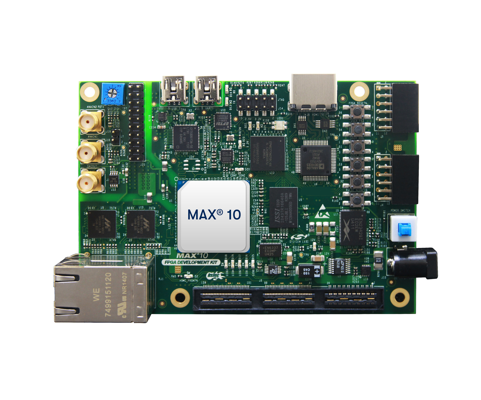
Thanks to its integrated flash configuration, single-supply voltage rail, and built-in ADC, the 10M16SAU169I7G requires minimal external components. A typical reference design includes a 3.3 V supply, decoupling capacitors, a JTAG header, and an optional external DDR3 SDRAM for data-intensive applications. Intel provides the MAX 10 FPGA Development Kit as a ready-to-use evaluation platform.
Design Checklist
- Power: Provide a clean 3.3 V rail (≥ 500 mA typical). The on-chip regulators generate 1.2 V core supply internally.
- Decoupling: Place 100 nF MLCC caps on every VCC ball and a bulk 10 µF capacitor near the device.
- JTAG: Connect TCK, TMS, TDI, TDO for programming via USB-Blaster or compatible.
- ADC inputs: Use a low-pass RC filter (100 Ω + 100 pF) on each analog channel for noise reduction.
- External memory: For DDR3 interfaces, follow Intel's board-design guidelines for trace impedance (50 Ω single-ended / 100 Ω differential).
Shop for development kits and accessories: FPGA development kits at wwdparts.com.
Video Tutorial: Getting Started with MAX 10 FPGA
FAQ – 10M16SAU169I7G
1. What is the difference between the 10M16SAU169I7G and 10M16SAU169C8G?
The "I7" suffix indicates the industrial temperature range (−40 °C to +100 °C) at speed grade 7, while the "C8" variant is rated for the commercial range (0 °C to +85 °C) at speed grade 8. Choose the I7G for harsh-environment or outdoor deployments.
2. Does the 10M16SAU169I7G require an external configuration flash?
No. MAX 10 FPGAs store their configuration in on-chip flash memory, enabling instant-on operation and eliminating the BOM cost and board area of an external PROM.
3. How many analog channels does the integrated ADC support?
The device includes a dual-channel 12-bit ADC capable of up to 1 MSPS. Up to 18 analog input pins can be multiplexed into the ADC block depending on the package variant. In the U169 package, the available analog channels are a subset of the full pin-out.
4. What development tools are needed?
Use Intel Quartus Prime Lite Edition (free) for synthesis, place-and-route, and JTAG programming. The Platform Designer (Qsys) tool lets you integrate soft-IP cores like Nios II processors, UARTs, SPI controllers, and memory interfaces.
5. Can I run a soft-core processor on the 10M16SAU169I7G?
Yes. With 16,000 LEs, the device comfortably hosts a Nios II/e (economy) or Nios II/f (fast) soft processor, leaving ample resources for custom peripherals and glue logic.
6. What external memory interfaces are supported?
The MAX 10 hard memory controller supports DDR2, DDR3, LPDDR2, and SRAM interfaces. In the U169 package, the available data-bus width depends on pin availability after allocating I/O for other functions.


