
10M16SAU169C8G Datasheet, Pinout & Specs | Intel MAX 10 FPGA Guide
The 10M16SAU169C8G is a non-volatile FPGA from Intel's (formerly Altera) MAX 10 family, built on a 55 nm flash process. It packs 16,000 logic elements, an integrated 12-bit ADC, and dual-image configuration flash into a compact 169-ball UBGA package—making it an ideal single-chip solution for industrial control, IoT edge nodes, motor drives, and sensor-interface designs that demand instant-on operation without external configuration memory.
Table of Contents
- Overview & Key Features
- Technical Specifications
- Block Diagram & Architecture
- Pinout & Package Information
- Application Circuit & Design Tips
- Frequently Asked Questions
Overview & Key Features
The Intel MAX 10 family revolutionized single-chip FPGA design by integrating non-volatile flash-based configuration on-die. The 10M16SAU169C8G eliminates the need for external EEPROM or SPI flash, enabling instant-on operation within milliseconds of power-up. Key highlights include:
- 16,000 Logic Elements – sufficient for complex state machines, communication bridges, and soft-core processors.
- Integrated 12-bit ADC – successive-approximation ADC with up to 18 analog input channels, supporting 1 MSPS throughput for direct sensor interface.
- Dual Configuration Images – remote system upgrade with automatic fail-safe fallback to the golden image.
- User Flash Memory (UFM) – 2,304 Kb of on-chip flash for data logging, calibration storage, or boot parameters.
- Single-Chip Solution – replaces multiple discrete components (CPLD + flash + ADC) on a single die, reducing BOM cost and board area.
Supported by Intel's free Quartus Prime Lite Edition, the 10M16SAU169C8G offers a cost-effective entry point for FPGA development with full synthesis, place-and-route, and Platform Designer (Qsys) system integration.
Technical Specifications
| Parameter | Value |
|---|---|
| Part Number | 10M16SAU169C8G |
| Manufacturer | Intel (Altera) |
| Family | MAX 10 FPGA |
| Process Technology | 55 nm Flash |
| Logic Elements (LEs) | 16,000 |
| Embedded Memory (M9K SRAM) | 549 Kb |
| User Flash Memory (UFM) | 2,304 Kb |
| 18 × 18 Multipliers | 45 |
| PLLs | 4 |
| ADC | 12-bit, up to 18 analog inputs, 1 MSPS |
| Maximum User I/O | 130 |
| Package | 169-UBGA (U169), 11 × 11 mm |
| Core Supply Voltage | 1.2 V |
| I/O Voltage Support | 3.3 V / 2.5 V / 1.8 V / 1.5 V |
| Speed Grade | C8G (Commercial) |
| Operating Temperature | 0 °C to 85 °C (TJ) |
| Configuration | Internal flash, dual-image, instant-on |
| Lead-Free / RoHS | Yes (Green / RoHS Compliant) |
Block Diagram & Architecture
The MAX 10 architecture combines a sea-of-LEs fabric with dedicated M9K memory blocks, DSP multipliers, PLLs, and an on-chip configuration flash controller. The block diagram below illustrates a typical system built around the 10M16SAU169C8G on a development board:
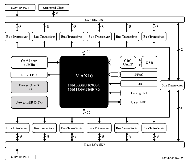
Block diagram of an Intel MAX 10 FPGA-based board featuring the 10M16SAU169C8G, showing the interconnection of logic fabric, embedded memory, ADC block, and external interfaces.
The integrated configuration flash controller manages dual-image storage and seamless fallback. During power-up, the device loads the active image in under 10 ms—no external boot ROM required. The on-die 12-bit ADC connects directly to analog input pins, simplifying mixed-signal designs.
Pinout & Package Information
The 10M16SAU169C8G ships in a 169-ball UBGA package measuring 11 × 11 mm with a 0.8 mm ball pitch. It provides up to 130 user I/O pins across multiple I/O banks, each independently configurable for 3.3 V, 2.5 V, 1.8 V, or 1.5 V operation.
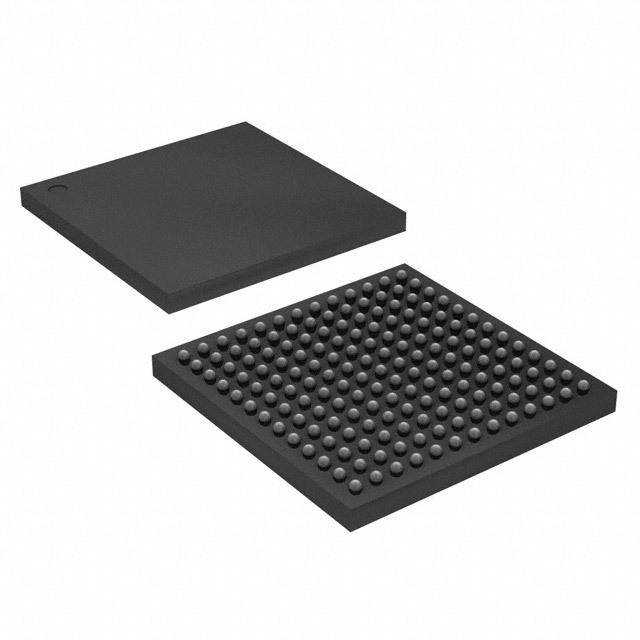
Physical view of the Intel 10M16SAU169C8G in its 169-UBGA package. Note the BGA ball array pattern and the Intel (Altera) part marking on the top side.
Pin Categories
- User I/O Pins – 130 general-purpose I/Os supporting LVTTL, LVCMOS, SSTL, HSTL, and differential standards.
- Analog Input Pins – dedicated analog pins routed to the internal 12-bit ADC.
- Configuration Pins – JTAG (TCK, TMS, TDI, TDO) for programming and boundary-scan testing.
- Power/Ground – VCC (1.2 V core), VCCIO (per bank), GND.
For the complete pinout table and recommended PCB landing pattern, download the official Intel 10M16SAU169C8G Pin-Out File (MDDS).
Application Circuit & Design Tips
The 10M16SAU169C8G excels in designs that need a compact, low-power programmable logic solution with mixed-signal capability. Common applications include:
- Industrial Sensor Hub – read multiple analog sensors via the built-in ADC, pre-process data in the FPGA fabric, and communicate over SPI/I2C/UART to a host MCU.
- Motor Control – implement PWM generators, encoder interfaces, and PID loops entirely in programmable logic with deterministic timing.
- IoT Edge Gateway – protocol bridging between legacy serial interfaces and modern Ethernet/Wi-Fi modules.
- Software-Defined Radio (SDR) – the LimeSDR-Mini uses the 10M16SAU169C8G as its FPGA backbone for digital signal processing.
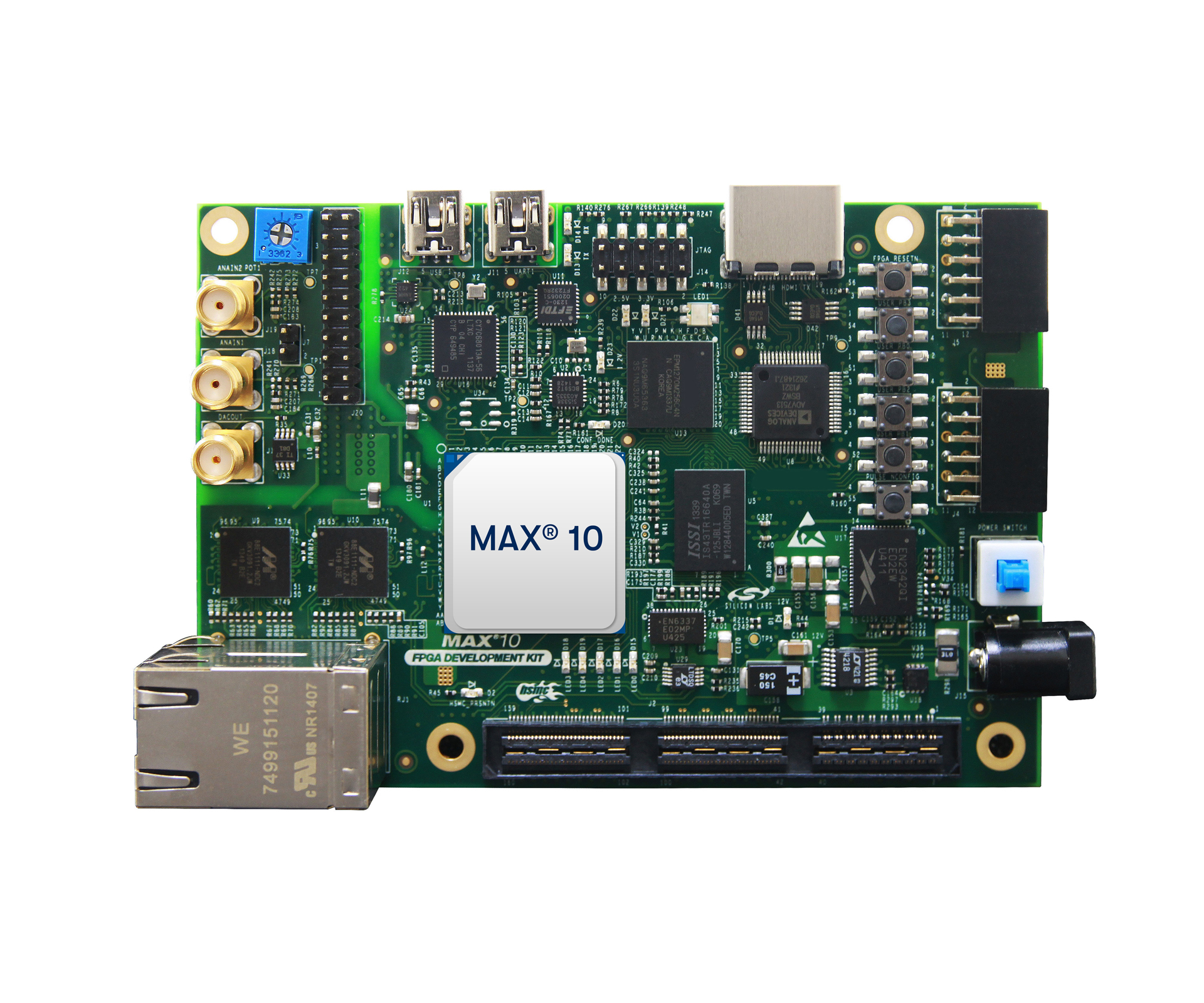
The Intel MAX 10 FPGA Development Kit provides a ready-to-use evaluation platform for prototyping designs around MAX 10 devices like the 10M16SAU169C8G.
Design Recommendations
- Power Sequencing – bring up VCC (1.2 V) before VCCIO banks. Use the POR (Power-On Reset) circuit to ensure clean startup.
- Decoupling – place 100 nF ceramic capacitors on every VCC and VCCIO pin, plus 10 µF bulk caps near the device.
- JTAG Routing – keep JTAG traces short and add series resistors (33 Ω) for signal integrity.
- ADC Reference – provide a clean, low-noise VREFADC supply for optimal 12-bit accuracy.
- Thermal Management – the U169 package has a low θJA; ensure adequate copper pour and airflow for designs exceeding 50% LE utilization.
Video: Getting Started with Intel MAX 10 FPGA
Related Intel MAX 10 FPGA Parts
- 10M16SAU169I7G – Industrial-temperature variant (-40 °C to 100 °C) of the same 16K LE / U169 device.
- 10M08SAE144C8G – 8,000 LE MAX 10 FPGA in a 144-pin EQFP package for space-constrained designs.
- IGLOO2 & SmartFusion2 FPGAs – alternative low-power FPGA families for comparison.
Frequently Asked Questions
What is the 10M16SAU169C8G?
The 10M16SAU169C8G is a non-volatile FPGA from Intel's MAX 10 family featuring 16,000 logic elements, an integrated 12-bit ADC, and dual-image configuration flash in a 169-ball UBGA package. It is designed for single-chip, instant-on applications in industrial, IoT, and consumer electronics.
Does the 10M16SAU169C8G require external configuration memory?
No. Unlike SRAM-based FPGAs, the MAX 10 stores its configuration in internal flash memory. The device powers up and becomes operational within milliseconds without any external EEPROM, SPI flash, or configuration controller.
What development tools support the 10M16SAU169C8G?
Intel's Quartus Prime Lite Edition (free, no license required) fully supports the MAX 10 family. It includes synthesis, place-and-route, timing analysis, the Platform Designer (Qsys) system integration tool, and the SignalTap II embedded logic analyzer for on-chip debugging.
Can the 10M16SAU169C8G be used for remote firmware updates?
Yes. The dual-image configuration flash supports remote system upgrade (RSU). You can update the application image over a communication link while the factory (golden) image serves as a fail-safe fallback, ensuring the device always boots even if an update is interrupted.
What is the operating temperature range of the 10M16SAU169C8G?
The C8G speed grade designates the commercial temperature range: 0 °C to 85 °C junction temperature. For extended or industrial temperature requirements (-40 °C to 100 °C), consider the 10M16SAU169I7G variant.
How many analog channels does the integrated ADC support?
The on-chip 12-bit successive-approximation ADC supports up to 18 analog input channels (dual ADC blocks with 9 channels each) at a maximum sampling rate of 1 MSPS. This enables direct sensor connectivity without an external ADC chip.


