
10M16SAU169I7G Datasheet, Specifications & Application Guide – Altera MAX 10 FPGA
The 10M16SAU169I7G is a non-volatile FPGA from the Altera (Intel) MAX 10 family, built on a 55 nm flash process. With 16,000 logic elements, an integrated dual 12-bit ADC, and internal configuration memory, the 10M16SAU169I7G delivers instant-on capability in a compact 169-ball UBGA package. This guide covers every parameter an engineer needs—from pinout and electrical specs to typical application circuits and design recommendations.
1. 10M16SAU169I7G Overview
The 10M16SAU169I7G belongs to the MAX 10 FPGA family originally developed by Altera, now part of Intel (Altera). MAX 10 devices are the industry's first single-chip, non-volatile FPGAs, integrating flash-based configuration storage that eliminates the need for an external configuration device. The "instant-on" power-up—with configuration completing in as little as 10 ms—makes the 10M16SAU169I7G ideal for industrial, automotive, and IoT edge applications where boot latency is critical.
Part number breakdown: 10M16 = MAX 10 with 16K LEs · S = single supply · A = analog block (dual ADC) · U169 = UBGA-169 package · I = industrial temperature (−40 °C to +100 °C) · 7 = speed grade 7. The device supports DDR3/DDR2/LPDDR2 external memory interfaces, up to 4 PLLs, and both single-ended and differential I/O standards including LVDS.
Whether you are designing a motor-drive controller, a sensor-fusion hub, or a compact video pre-processing pipeline, the 10M16SAU169I7G offers a cost-effective, single-chip solution. For related MAX 10 parts and cross-references, browse the wwdparts FPGA catalog.
2. Key Specifications & Parameters
| Parameter | Value |
|---|---|
| Manufacturer | Altera (Intel) |
| Family | MAX 10 FPGA |
| Part Number | 10M16SAU169I7G |
| Logic Elements (LEs) | 16,000 |
| Logic Array Blocks (LABs) | 1,000 |
| Embedded SRAM | 549 Kb |
| User Flash Memory (UFM) | 2,304 Kb |
| 18 × 18 Multipliers | 45 |
| PLLs | 4 |
| Maximum User I/Os | 130 (U169 package) |
| Maximum LVDS Pairs | 22 |
| Analog-to-Digital Converter | Dual 12-bit, up to 1 MSPS |
| Configuration Memory | Internal flash (instant-on) |
| External Memory Interfaces | DDR3, DDR2, LPDDR2, SRAM |
| I/O Standards | 3.3 V / 2.5 V / 1.8 V / 1.5 V LVCMOS, LVTTL, SSTL, HSTL, HSUL, LVDS, Mini-LVDS, RSDS |
| Core Voltage | 1.2 V |
| I/O Supply Voltage | 3.0 V – 3.3 V |
| Process Technology | 55 nm (flash-based) |
| Package | UBGA-169 (11 × 11 mm) |
| Mounting Type | SMD / SMT |
| Operating Temperature | −40 °C to +100 °C (Industrial) |
| Speed Grade | 7 |
| FPGA Bitstream Security | AES-256 encryption |
| Moisture Sensitivity Level | MSL-3 |
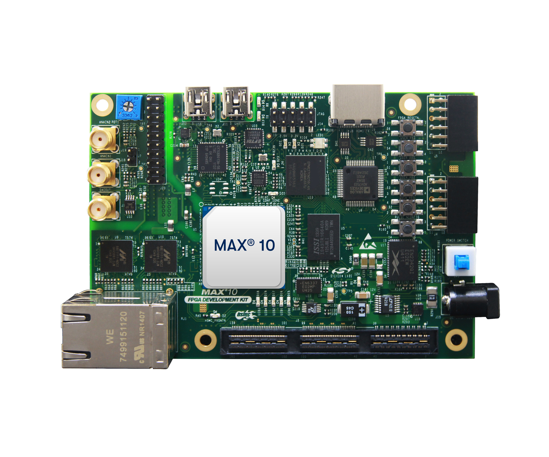
3. Block Diagram & Architecture
The MAX 10 architecture integrates logic array blocks, embedded memory, DSP blocks with 18 × 18 multipliers, a dual 12-bit ADC, four PLLs, and internal flash configuration memory into a single monolithic die. The block diagram below illustrates the system-level interconnect of a MAX 10 evaluation platform featuring the 10M16SAU169I7G FPGA at its core.
The 1,000 LABs are organized into rows and columns with a column-based routing fabric. Each LAB contains 16 adaptive logic modules (ALMs) that can implement combinational or registered functions. The four PLLs support frequency synthesis from 5 MHz to 472.5 MHz, while the integrated ADC block provides dual 12-bit channels with up to 17 analog input pins—critical for mixed-signal sensor-interface designs.
4. Pinout & Package Information
The 10M16SAU169I7G is housed in a 169-ball Ultra-Fine-Pitch BGA (UBGA) package with a 0.8 mm ball pitch and an 11 × 11 mm body size. The compact footprint makes it well-suited for space-constrained PCB layouts in handheld instruments, wearables, and small-form-factor IoT gateways.

Key pin groups include: VCCIO banks (3.3 V / 2.5 V / 1.8 V), VCCINT (1.2 V core), VCCA (PLL analog supply), GCLK global clock inputs, JTAG (TCK/TMS/TDI/TDO), and dedicated ADC analog input pins (ANAIN1–ANAIN17). Designers should follow the Altera power delivery guidelines and place decoupling capacitors within 2 mm of each VCC ball to ensure clean power delivery and minimize jitter on the PLL outputs.
5. Typical Application Circuits
The 10M16SAU169I7G is deployed across a wide range of embedded applications. Its integrated ADC and instant-on flash configuration make it a natural fit for industrial control, motor drives, sensor hubs, and video pre-processing pipelines. Below is the MAX 10 FPGA Development Kit—a reference platform that demonstrates the device in a complete system context with DDR3 memory, Ethernet, USB-Blaster II, and expansion headers.
Common Application Areas
- Industrial Motor Control: Real-time PWM generation, encoder interfaces, and integrated ADC for current sensing—all in a single 10M16SAU169I7G device.
- IoT Sensor Hub: The dual 12-bit ADC samples temperature, humidity, and pressure sensors while the FPGA fabric implements Kalman filtering and SPI/I²C bridging.
- Video Pre-Processing: Parallel camera interfaces feed pixel data through Bayer-to-RGB conversion and scaling pipelines implemented in the 16K LE fabric.
- Medical Instrumentation: Instant-on configuration ensures patient-monitoring devices are operational within milliseconds of power-up, meeting IEC 62304 boot-time requirements.
For power supply design, a typical single-supply configuration uses an LDO or DC-DC converter to generate the 1.2 V core rail from a 3.3 V input. The device's single-supply variant (S designation) simplifies the power tree. Explore more semiconductor components at wwdparts.
Video Tutorial: Getting Started with MAX 10 FPGA
6. Frequently Asked Questions
What is the 10M16SAU169I7G?
The 10M16SAU169I7G is a non-volatile FPGA from the Altera MAX 10 family featuring 16,000 logic elements, an integrated dual 12-bit ADC, and internal flash configuration memory in a 169-ball UBGA package rated for industrial temperatures (−40 °C to +100 °C).
What software is needed to program the 10M16SAU169I7G?
Intel Quartus Prime Lite Edition (free) supports all MAX 10 devices. It provides synthesis, place-and-route, timing analysis, and JTAG-based programming via USB-Blaster or USB-Blaster II. Designs can be entered in Verilog, VHDL, or schematic capture.
Does the 10M16SAU169I7G require an external configuration flash?
No. MAX 10 FPGAs integrate on-chip flash configuration memory, enabling instant-on operation without any external EEPROM or SPI flash. The device configures itself in approximately 10 ms after power-up.
What is the maximum operating frequency of the 10M16SAU169I7G?
The four integrated PLLs support output frequencies up to 472.5 MHz. The internal logic fabric typically achieves 200–300 MHz Fmax depending on design complexity and the speed grade 7 timing characteristics.
Can the 10M16SAU169I7G interface with DDR3 memory?
Yes. The MAX 10 family includes hard memory controller support for DDR3, DDR2, LPDDR2, and SRAM interfaces. The EMIF IP core in Quartus Prime configures the PHY and controller for common memory densities and speeds.
What is the difference between 10M16SAU169I7G and 10M16SAU169C8G?
Both share the same 16K LE die in the UBGA-169 package. The key differences are: the I7G variant is industrial-grade (−40 °C to +100 °C) with speed grade 7, while the C8G is commercial-grade (0 °C to +85 °C) with speed grade 8. The I7G is preferred for applications exposed to extended temperature ranges.


