
10M16SAU169I7G Altera MAX 10 FPGA: Datasheet, Pinout, and Application Guide
Overview of the 10M16SAU169I7G
The 10M16SAU169I7G is a non-volatile FPGA from Altera's (now Intel) MAX 10 family, built on a 55nm flash process. This device integrates 16,000 logic elements, a dual 12-bit analog-to-digital converter (ADC), and internal flash configuration memory into a compact 169-ball UBGA package. The "S" in the part number denotes single power-supply operation, while "A" indicates the ADC-enabled variant, making the 10M16SAU169I7G one of the most integrated non-volatile FPGAs available in its class.
Unlike traditional FPGAs that require external configuration devices, the MAX 10 family stores its configuration bitstream in on-chip flash memory. This enables instant-on operation with power-on times under 10 milliseconds, eliminating the boot-up latency associated with external serial flash loading. The dual configuration flash also supports remote field updates with a fail-safe fallback image, ensuring high system availability.
The 10M16SAU169I7G is rated for the industrial temperature range (-40°C to +100°C) with speed grade 7, making it suitable for harsh-environment deployments in industrial automation, IoT edge computing, sensor interface systems, motor control, and embedded instrumentation. Its combination of analog sensing (ADC), digital processing (FPGA logic and DSP), and non-volatile storage in a single chip significantly reduces board space and BOM cost compared to multi-chip alternatives. Find compatible FPGA devices at wwdparts.com FPGA collection.
Key Specifications and Parameters
| Parameter | Value |
|---|---|
| Manufacturer | Altera (Intel) |
| Family | MAX 10 (10M16) |
| Part Number | 10M16SAU169I7G |
| Logic Elements (LEs) | 16,000 |
| Logic Array Blocks (LABs) | 1,000 |
| Embedded SRAM | 549 Kb (M9K blocks) |
| User Flash Memory (UFM) | 2,304 Kb |
| 18x18 DSP Multipliers | 45 |
| Fabric and I/O PLLs | 4 |
| Analog-to-Digital Converter | Dual 12-bit ADC, up to 1 MSPS |
| Maximum User I/O (U169) | 130 |
| Package Type | 169-ball UBGA (11 x 11 mm, 0.8mm pitch) |
| Core Supply Voltage | 1.2V |
| I/O Supply Voltage | 3.0V / 3.3V |
| I/O Standards | LVTTL, LVCMOS (1.2V–3.3V), PCI, SSTL, HSTL, HSUL, LVDS |
| Operating Temperature | -40°C to +100°C (Industrial) |
| Speed Grade | 7 |
| Process Technology | 55nm Flash |
| Configuration Memory | Internal flash (dual image, instant-on) |
| External Memory Support | DDR2, DDR3, LPDDR2, SRAM |
| LVDS Pairs | Up to 22 |
| Mounting Type | Surface Mount (SMD/SMT) |
| RoHS Compliance | Yes (Lead-Free, "G" suffix) |
| Product Status | Active |
The 10M16SAU169I7G offers 45 embedded 18x18 DSP multiplier blocks that support efficient implementation of digital filters, math functions, and signal processing algorithms. The dual 12-bit ADC with up to 17 analog input channels can sample at up to 1 MSPS, enabling direct sensor interfacing without external ADC chips. The 2,304 Kb of user flash memory provides non-volatile on-chip storage for calibration data, coefficients, or system parameters. For related MAX 10 components, browse the Altera parts catalog at WWDParts.
Block Diagram and Architecture
The MAX 10 architecture in the 10M16SAU169I7G is organized around a regular array of logic array blocks (LABs), each containing 16 adaptive look-up tables (ALUTs) and associated registers. The FPGA fabric is surrounded by configurable I/O elements, M9K embedded memory blocks, DSP multiplier blocks, and phase-locked loops (PLLs) that provide clock management and frequency synthesis.
Key architectural highlights include:
- Internal Configuration Flash Memory: Dual configuration flash images allow seamless remote updates with automatic fallback. The device boots from flash in under 10 ms, enabling true instant-on behavior without an external configuration PROM.
- Dual 12-bit ADC: Two successive-approximation-register (SAR) ADCs share up to 17 analog input channels with a dedicated analog-to-digital converter block (ADCBLOCK). Each ADC channel supports single-ended inputs with built-in temperature sensing and voltage monitoring.
- M9K Embedded Memory: The 549 Kb of embedded SRAM is organized in M9K blocks (9,216 bits each), supporting true dual-port, single-port, ROM, and FIFO configurations with independent read/write clocks and optional parity bits.
- DSP Blocks: 45 embedded 18x18 multipliers support multiply-accumulate (MAC) operations for FIR/IIR filters, FFTs, and matrix operations, freeing logic elements for other functions.
Pinout and Package Information
The 10M16SAU169I7G is housed in a 169-ball Ultra-thin Fine-pitch Ball Grid Array (UBGA) with an 11mm x 11mm body size and 0.8mm ball pitch. The compact form factor makes it ideal for space-constrained designs while providing 130 user I/O pins organized across multiple I/O banks. The U169 package supports a wide range of single-ended and differential I/O standards, including up to 22 LVDS differential pairs for high-speed data transfer.

The I/O pins are organized into banks that can be individually configured for different voltage levels (1.2V, 1.5V, 1.8V, 2.5V, 3.0V, 3.3V). Dedicated pins include JTAG (TCK, TMS, TDI, TDO) for boundary-scan testing and in-system programming, analog input channels for the dual ADC, and clock input pins connected to the four on-chip PLLs. The single power-supply feature ("S" variant) simplifies the power delivery network by requiring only a 3.3V external supply, with the on-chip voltage regulator generating the 1.2V core voltage internally.
For complete pin assignment tables, footprint dimensions, and PCB landing pattern recommendations, consult the IC product pages at WWDParts.
Application Circuit and Design Guide
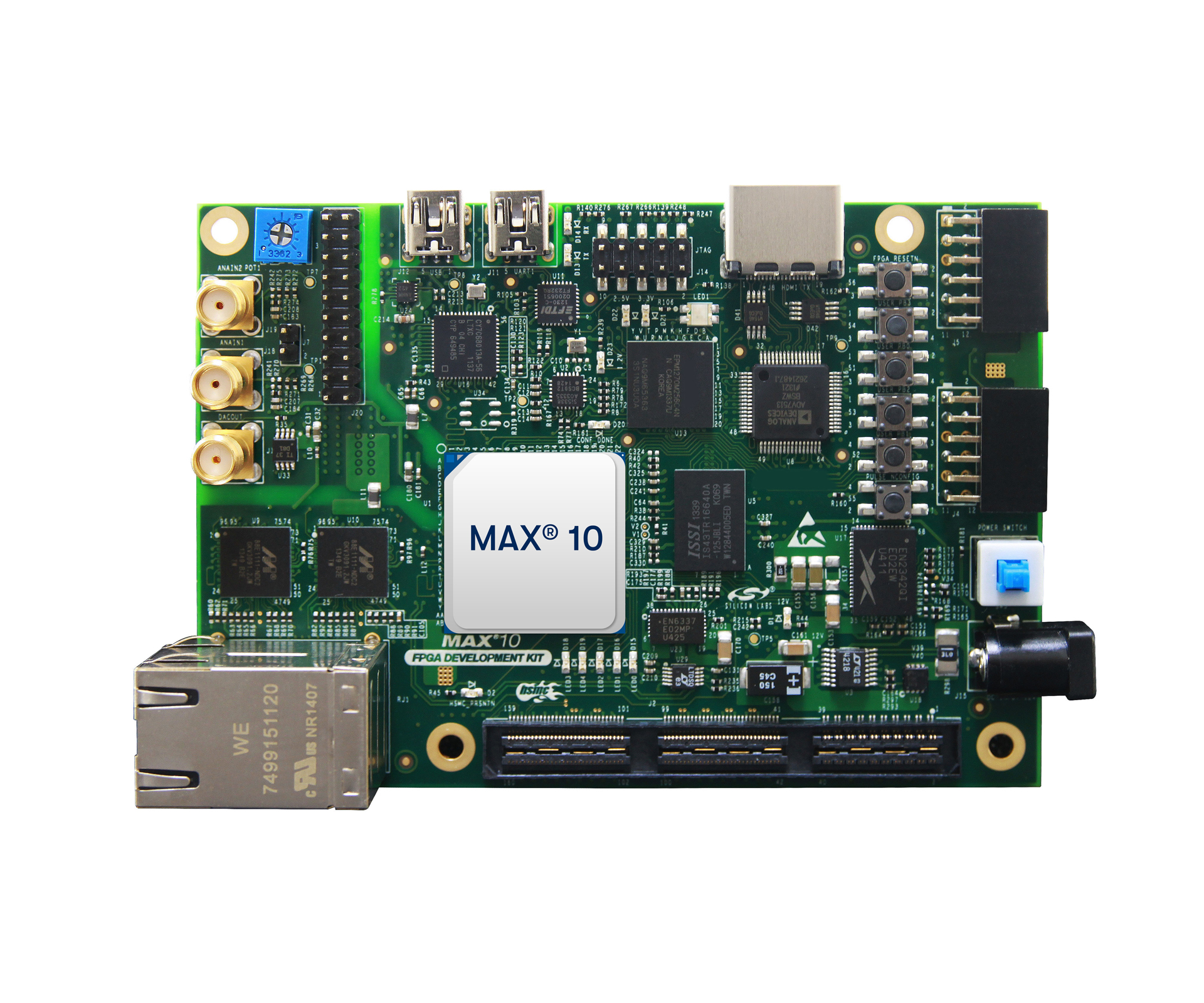
The 10M16SAU169I7G excels in applications that benefit from its integrated ADC, instant-on flash configuration, and compact UBGA package. The MAX 10 FPGA Development Kit provides a full-featured evaluation platform with onboard DDR3 SDRAM, HSMC expansion, and analog input headers for rapid prototyping with the 10M16 device family.
Design guidelines for the 10M16SAU169I7G:
- Power Supply Design: The single-supply "S" variant simplifies power by requiring only a 3.3V input. An internal regulator generates the 1.2V core supply. Add 10uF bulk and 100nF local bypass capacitors at each VCC pin. For the "D" (dual-supply) variant, an external 1.2V regulator is needed for VCCINT.
- ADC Interfacing: Provide a clean analog supply (VCCADC = 2.5V) with dedicated filtering. Route analog input traces away from digital switching signals. The ADC supports a 0V to 2.5V input range with built-in prescaler for wider voltage monitoring.
- Configuration: The internal flash stores up to two configuration images. Use the Quartus Prime Programmer to load images via JTAG. For in-field updates, implement a remote update controller IP to manage dual-image switching with automatic error recovery.
- DDR3 Memory Interface: The MAX 10 hard memory controller supports DDR3 at up to 300 MHz (600 Mbps data rate). Follow Intel's recommended PCB stackup and routing guidelines for impedance matching and signal integrity.
Development is fully supported by the free Quartus Prime Lite Edition, which includes synthesis, place-and-route, timing analysis, and the Platform Designer (Qsys) system integration tool. The Nios II soft processor can be instantiated in the FPGA fabric for embedded software development.
Video Tutorial: Getting Started with MAX 10 FPGA
Frequently Asked Questions
What is the 10M16SAU169I7G and what FPGA family does it belong to?
The 10M16SAU169I7G is a non-volatile FPGA from the Altera (Intel) MAX 10 family. It features 16,000 logic elements, a dual 12-bit ADC, 549 Kb embedded SRAM, 2,304 Kb user flash memory, and 45 DSP multiplier blocks in a 169-ball UBGA package. The MAX 10 family is unique among FPGAs for integrating internal flash configuration memory, enabling instant-on operation without external configuration devices.
What does each segment of the 10M16SAU169I7G part number mean?
The part number breaks down as follows: 10M = MAX 10 family, 16 = 16,000 logic elements, S = single power-supply (internal 1.2V regulator), A = ADC-enabled variant, U169 = 169-ball UBGA package, I = industrial temperature range (-40°C to +100°C), 7 = speed grade 7, G = lead-free (RoHS compliant) packaging.
Does the 10M16SAU169I7G require an external configuration memory?
No. The 10M16SAU169I7G stores its configuration bitstream in internal flash memory, eliminating the need for external serial configuration PROMs or flash chips. The device powers on and configures in under 10 milliseconds. It supports dual configuration images for fail-safe remote updates: if a new image fails to load, the device automatically reverts to the backup image.
What are the ADC capabilities of the 10M16SAU169I7G?
The 10M16SAU169I7G integrates a dual 12-bit successive-approximation-register (SAR) ADC block that supports up to 17 analog input channels with a maximum sample rate of 1 MSPS. The ADC accepts 0V to 2.5V single-ended inputs with built-in temperature sensor and internal voltage reference. An optional prescaler circuit enables monitoring of voltages up to the VCCIO level. The ADC is controlled through a soft IP core instantiated in the FPGA fabric.
What software tools are needed to program the 10M16SAU169I7G?
The 10M16SAU169I7G is supported by the free Quartus Prime Lite Edition from Intel/Altera, which includes RTL synthesis, place-and-route, timing analysis, and the built-in JTAG programmer. The Platform Designer (formerly Qsys) enables system-level integration of IP cores including the Nios II soft processor, DDR3 memory controller, ADC interface, and various peripheral controllers. No paid license is required for MAX 10 devices.
What are the key differences between the 10M16SAU169I7G and the 10M16SAU169C8G?
Both devices share the same 16,000 LE MAX 10 architecture in the U169 package, but they differ in temperature range and speed grade. The I7G variant operates across the full industrial range (-40°C to +100°C) at speed grade 7, while the C8G is rated for the commercial range (0°C to 85°C) at speed grade 8. The I7G is preferred for industrial, outdoor, and harsh-environment applications where extended temperature tolerance is critical.


