
10M08SAE144C8G Datasheet, Pinout, Specifications & Application Guide | Intel MAX 10 FPGA
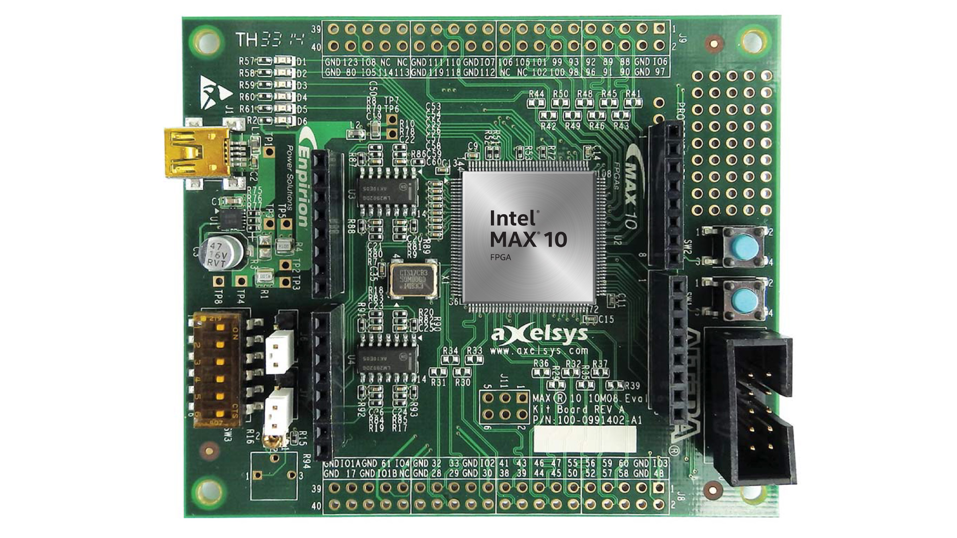
The 10M08SAE144C8G is an Intel (formerly Altera) MAX 10 FPGA built on 55nm flash process technology. It delivers 8,000 logic elements, an integrated 12-bit ADC, and dual configuration flash memory in a compact 144-pin EQFP package. Ideal for embedded processing, industrial automation, and IoT edge devices, the 10M08SAE144C8G provides instant-on capability, single-chip integration, and cost-effective FPGA performance without external configuration memory.
Table of Contents
- 1. Device Overview & Key Features
- 2. Technical Specifications & Parameters
- 3. Pinout & Package Information
- 4. Block Diagram & Architecture
- 5. Application Circuits & Design Guide
- 6. Frequently Asked Questions (FAQ)
1. Device Overview & Key Features
The 10M08SAE144C8G belongs to Intel's MAX 10 FPGA family — the industry's first single-chip, non-volatile FPGA with integrated analog features. The "SA" designation indicates it is a single-supply analog variant, meaning the on-chip ADC operates from a single 3.3 V power rail, eliminating the need for a separate analog supply.
Key advantages of the 10M08SAE144C8G include:
- Instant-On: Internal flash configuration boots the device in under 10 ms — no external EPROM or SPI flash needed.
- Integrated ADC: A 12-bit, 1 MSPS SAR ADC with up to 18 analog input channels enables direct sensor interfacing.
- Dual Configuration Flash: Store two design images on-chip for remote update with safe fallback.
- User Flash Memory: Up to 172 KB of on-chip user flash for non-volatile data storage.
- Nios II Soft Processor: Implement an embedded CPU core entirely within the FPGA fabric.
- Free Toolchain: Fully supported by Quartus Prime Lite Edition (no license required).
2. Technical Specifications & Parameters
| Parameter | Value |
|---|---|
| Manufacturer | Intel (Altera) |
| Family | MAX 10 (10M08) |
| Part Number | 10M08SAE144C8G |
| Logic Elements (LE) | 8,000 |
| Embedded Memory (M9K) | 378 Kb (42 M9K blocks) |
| User Flash Memory | 32 KB – 172 KB |
| 18×18 Multipliers | 24 |
| PLLs | 2 |
| ADC | 1× 12-bit SAR, 1 MSPS, up to 18 channels |
| User I/O Pins | 101 |
| Package | 144-EQFP (20 mm × 20 mm, 0.5 mm pitch) |
| Core Voltage (VCCINT) | 1.2 V |
| I/O Voltage (VCCIO) | 1.0 V – 3.3 V (multi-bank) |
| I/O Standards | 3.3 V LVTTL, LVCMOS, SSTL, HSTL, LVDS |
| Process Technology | 55 nm flash (TSMC) |
| Speed Grade | C8 (commercial, –40 °C to +85 °C) |
| Configuration | Internal dual-image flash, JTAG |
| Operating Temperature | –40 °C to +85 °C (commercial) |
| RoHS Compliant | Yes (Pb-free, "G" suffix) |
3. Pinout & Package Information
The 10M08SAE144C8G uses a 144-pin Enhanced Quad Flat Package (EQFP) with an exposed thermal pad on the underside. The package measures 20 mm × 20 mm with a 0.5 mm lead pitch. The 101 user I/O pins are organized across multiple I/O banks, each of which can be independently configured for different voltage standards.

Key pin groups include:
- VCCINT (1.2 V): Core logic supply — connect all VCCINT pins with adequate decoupling capacitors.
- VCCIO (per bank): Independent I/O bank supply, configurable from 1.0 V to 3.3 V.
- VCCA / GND_ADC: Dedicated analog supply and ground for the integrated ADC block.
- JTAG (TCK, TDI, TDO, TMS): Programming and debug interface.
- Exposed Pad (GND): Must be soldered to the ground plane for optimal thermal and electrical performance.
4. Block Diagram & Architecture
The MAX 10 architecture follows a column-based structure. Logic Array Blocks (LABs) — each containing 16 Adaptive Logic Modules (ALMs) — are arranged in columns alongside M9K memory blocks and 18×18 multiplier DSP blocks. Two PLLs provide flexible clock synthesis and phase shifting.

The integrated Configuration Flash Memory (CFM) stores up to two FPGA images, enabling:
- Dual-image boot: Application image + factory fallback image for safe remote updates.
- Instant-on: Device configures from internal flash in < 10 ms at power-up.
- User Flash Memory (UFM): Remaining flash capacity is available for non-volatile data storage accessible at runtime.
The on-chip ADC block connects to dedicated analog input pins and includes a temperature-sensing diode, enabling on-die thermal monitoring without external components.
5. Application Circuits & Design Guide
The 10M08SAE144C8G is well-suited for a wide range of applications thanks to its combination of logic, analog, and flash resources in a single chip:
- Industrial IoT Edge Nodes: Use the ADC to digitize sensor data, process it in FPGA logic, and transmit over SPI/UART/I²C to a wireless module.
- Motor Control: Implement PWM generators, encoder interfaces, and PID controllers with deterministic timing impossible in MCU firmware.
- LED Display Controllers: Drive multiplexed LED panels with precise timing using hard logic — no CPU overhead.
- Protocol Bridges: Convert between UART, SPI, I²C, LVDS, and parallel buses in real time.
- Education & Prototyping: The free Quartus toolchain and low-cost eval boards make MAX 10 ideal for learning digital design.
Power Supply Design Tips:
- Provide a clean 1.2 V rail for VCCINT with low-ESR capacitors (100 nF MLCC per pin pair + 10 µF bulk).
- Use separate VCCIO regulators per I/O bank if mixing voltage standards.
- Route VCCA through a ferrite bead or LC filter for best ADC performance.
- Connect the exposed thermal pad to a solid ground plane with multiple vias.
6. Frequently Asked Questions (FAQ)
What is the 10M08SAE144C8G?
The 10M08SAE144C8G is an Intel MAX 10 FPGA with 8,000 logic elements, an integrated 12-bit ADC, and dual configuration flash memory in a 144-pin EQFP package. It is a single-supply analog variant designed for cost-sensitive embedded and industrial applications.
Does the 10M08SAE144C8G require external configuration memory?
No. The MAX 10 family stores its configuration bitstream in on-chip flash memory. The 10M08SAE144C8G supports dual-image storage, enabling instant-on boot in under 10 ms without any external EPROM or SPI flash.
What is the difference between 10M08SAE144C8G and 10M08DAF256C8G?
Both share the same 8,000 LE MAX 10 die. The key differences are: the 10M08SAE144C8G uses a 144-pin EQFP package with 101 I/Os and a single analog supply, while the 10M08DAF256C8G uses a 256-pin FBGA package with more I/Os and a dual analog supply supporting two independent ADC blocks.
What development tools support the 10M08SAE144C8G?
Intel Quartus Prime Lite Edition (free, no license required) fully supports the MAX 10 family. It includes the Quartus synthesizer, ModelSim simulator, Platform Designer (Qsys) for system integration, and the Nios II soft-processor IDE. Programming is done via USB-Blaster JTAG.
How many ADC channels does the 10M08SAE144C8G have?
The 10M08SAE144C8G integrates one ADC block (single-supply analog variant) providing a 12-bit SAR ADC running at up to 1 MSPS. It supports up to 18 analog input channels, including a built-in temperature-sensing diode for on-die thermal monitoring.
What is the operating temperature range of the 10M08SAE144C8G?
The "C8" speed grade designation indicates commercial temperature range: –40 °C to +85 °C. For extended or industrial temperature ranges, Intel offers "I7" variants (–40 °C to +100 °C) of the same MAX 10 die.


