
Request a Quote · 10M16SAU169C8G
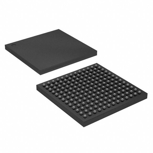
10M16SAU169C8G Package and Pinout Reference
The 10M16SAU169C8G is a non-volatile FPGA from Intel's (formerly Altera) MAX 10 family, built on 55 nm flash process technology. Housed in a compact 169-ball UBGA package, it delivers 16,000 logic elements, 549 Kb of embedded SRAM, 2,304 Kb of user flash memory, and an integrated 12-bit ADC — all within a single chip that requires no external configuration memory. Its instant-on capability and single-supply operation make it a practical choice for industrial automation, sensor aggregation, motor control, and protocol bridging applications.
Table of Contents
1. Overview and Core Features
The 10M16SAU169C8G belongs to the Intel MAX 10 FPGA family, which combines flash-based non-volatile configuration storage with FPGA programmability. Unlike SRAM-based FPGAs that require external flash or EEPROM for configuration, MAX 10 devices store their configuration internally in on-chip flash, enabling instant-on operation within milliseconds of power-up.
Key features of the 10M16SAU169C8G include:
- 16,000 Logic Elements (LEs): Sufficient for mid-complexity digital designs including state machines, data pipelines, and protocol converters.
- Dual Configuration Images: Supports remote update with fail-safe fallback, allowing field upgrades without risk of bricking the device.
- Integrated 12-bit ADC: A successive-approximation ADC with up to 18 analog input channels eliminates the need for external ADC ICs in mixed-signal designs.
- User Flash Memory (UFM): 2,304 Kb of on-chip flash for storing calibration data, encryption keys, or user-defined parameters.
- Single-Supply Operation: Operates from a single 1.2 V core supply, simplifying power supply design.
- SEU Immunity: Single event upset immunity from flash-based configuration, critical for industrial and outdoor deployments.
2. Specifications and Parameter Table
| Parameter | Value |
|---|---|
| Part Number | 10M16SAU169C8G |
| Manufacturer | Intel (Altera) |
| Family | MAX 10 |
| Logic Elements (LEs) | 16,000 |
| Embedded SRAM (M9K) | 549 Kb |
| User Flash Memory (UFM) | 2,304 Kb |
| 18x18 Multipliers | 45 |
| PLLs | Up to 4 |
| ADC | 12-bit SAR, up to 18 channels |
| Max User I/O | 130 |
| Package | 169-UBGA (11 mm x 11 mm) |
| Core Voltage | 1.2 V |
| Speed Grade | C8G (Commercial, 0°C to 85°C) |
| Process Technology | 55 nm Flash |
| Configuration | Internal (dual boot images) |
| I/O Standards | LVTTL, LVCMOS, SSTL, HSTL, LVDS |
Looking for 10M16SAU169C8G Inventory?
Check our real-time stock levels, pricing, and volume discounts for global distribution.
Check 10M16SAU169C8G Stock3. Architecture and Block Diagram
The MAX 10 FPGA architecture is organized around adaptive logic modules (ALMs) interconnected through a columnar routing fabric. Each logic element contains a 4-input look-up table (LUT), a programmable register, and dedicated carry chain logic. The 10M16SAU169C8G integrates these logic resources alongside embedded memory blocks (M9K), DSP blocks with 18x18 multipliers, and a global clock network fed by up to 4 PLLs.

Intel MAX 10 FPGA Architecture Block Diagram
The integrated 12-bit ADC block connects directly to the FPGA fabric, enabling low-latency analog signal acquisition without external components. Eight I/O banks surround the logic core, each independently configurable for different voltage standards (1.2 V to 3.3 V), providing flexibility when interfacing with diverse peripherals on the same board.
4. Video: Intel MAX 10 FPGA Tutorial
5. Equivalents, Cross-Reference, and Lifecycle
The 10M16SAU169C8G is an active-production device supported by Quartus Prime Lite Edition (free). For designers evaluating alternatives within the MAX 10 family or considering migration paths, the following cross-reference data is relevant:
- 10M16SAU169I7G: Industrial-temperature variant (-40°C to 100°C) of the same device, same pinout and logic capacity. Direct drop-in replacement for extended-temperature applications.
- 10M08SAE144C8G: A lower-density MAX 10 option with 8,000 LEs in a 144-EQFP package. Suitable when fewer logic resources are required and through-hole prototyping is preferred.
- 10M25SAE144C8G: Higher-density MAX 10 variant with 25,000 LEs, for designs that outgrow the 16K LE capacity.

Intel MAX 10 FPGA-Based Development Board — Typical Application Circuit
The MAX 10 family remains in active production with long-term supply commitments from Intel. Quartus Prime Lite provides full synthesis, simulation, and programming support at no cost, making the 10M16SAU169C8G accessible for both prototyping and volume production.
6. Frequently Asked Questions (FAQ)
Q1: Does the 10M16SAU169C8G require external configuration memory?
No. The 10M16SAU169C8G stores its configuration in on-chip flash memory, eliminating the need for external EEPROM or flash ICs. The device boots from internal flash within milliseconds of power-up, enabling true instant-on operation.
Q2: What is the operating temperature range of the 10M16SAU169C8G?
The C8G suffix designates the commercial temperature grade, operating from 0°C to 85°C. For industrial applications requiring -40°C to 100°C, the pin-compatible 10M16SAU169I7G is available.
Q3: How many analog inputs does the integrated ADC support?
The 10M16SAU169C8G features an integrated 12-bit successive-approximation ADC that supports up to 18 single-ended analog input channels. The ADC operates at up to 1 MSPS and connects directly to the FPGA fabric for low-latency data acquisition.
Q4: What software is needed to program the 10M16SAU169C8G?
Intel Quartus Prime Lite Edition (free, no license required) fully supports the MAX 10 family. It includes synthesis, place-and-route, timing analysis, and the Quartus Prime Programmer for JTAG configuration. ModelSim-Intel Starter Edition provides RTL simulation.
Q5: Can the 10M16SAU169C8G support remote firmware updates?
Yes. The dual configuration image feature allows the device to store two separate FPGA configurations in on-chip flash. During a remote update, the new image is written to the secondary slot. If the update fails or the new image is corrupt, the device automatically falls back to the known-good primary image.
Q6: What are the main differences between the 10M16SAU169C8G and the 10M08SAE144C8G?
The 10M16SAU169C8G provides 16,000 LEs, 549 Kb embedded SRAM, and 130 user I/O in a 169-UBGA package. The 10M08SAE144C8G offers 8,000 LEs, 378 Kb embedded SRAM, and 101 user I/O in a 144-EQFP package. The 10M16 variant is better suited for designs requiring more logic density and I/O count, while the 10M08 in EQFP is easier to hand-solder for prototyping.
Alan Carter, Senior Hardware Engineer
Alan has over 15 years of experience in embedded systems design, specializing in ARM Cortex architectures, PCB routing for high-speed digital signals, and industrial IoT deployments. He frequently contributes technical teardowns and architecture comparisons.


