XC7Z030-1FBG676C Application Guide: From Datasheet to Working Circuit
When designing a high-channel-count data acquisition (DAQ) system for applications like medical imaging or advanced wireless testbeds, the challenge lies in capturing, processing, and managing massive data streams in real-time. The Xilinx XC7Z030-1FBG676C, a member of the Zynq-7000 All Programmable SoC family, is purpose-built for this task. It uniquely handles the high-speed, parallel data ingestion and pre-processing in its Programmable Logic (PL) fabric, while its dual-core ARM Cortex-A9 Processing System (PS) manages complex algorithms, network communication, and system control, all within a single device.

Table of Contents
Application Context: Where XC7Z030-1FBG676C Fits in the System
In a modern multi-channel DAQ system, the XC7Z030-1FBG676C acts as the central processing hub. Imagine a system designed to interface with eight high-speed Analog-to-Digital Converters (ADCs), each sampling at 125 MSPS with 14-bit resolution. The sheer volume of raw data—1.75 Gigabytes per second (8 channels * 125 MSPS * 14 bits / 8 bits/byte)—is too much for a conventional microcontroller to handle directly. This is where the Zynq architecture excels.
The system block diagram places the XC7Z030 at the core. The high-speed LVDS or parallel CMOS outputs from the eight ADCs are routed directly to the I/O banks of the Zynq's Programmable Logic (PL) section. Inside the PL, we instantiate eight parallel data capture modules. Each module deserializes the incoming data (if LVDS) and feeds it into a dedicated digital signal processing (DSP) pipeline. This pipeline might consist of a digital down-converter (DDC), a polyphase decimating FIR filter to reduce the sample rate and filter out-of-band noise, and a data-width converter. The use of the PL's fabric and dedicated DSP48E1 slices allows this front-end processing to occur simultaneously on all eight channels with deterministic, low latency.
Once pre-processed, the reduced-rate data from all channels is aggregated and buffered in the PL's internal Block RAM (BRAM). A central AXI Direct Memory Access (DMA) controller, also implemented in the PL, then efficiently transfers these data blocks into the main system DDR3 memory, which is connected to the Processing System (PS). This transfer happens over the high-bandwidth AXI interconnect, a key feature of the Zynq architecture that tightly couples the PL and PS.
Meanwhile, the dual-core ARM Cortex-A9 processor in the PS is running a real-time operating system (RTOS) or a lightweight embedded Linux distribution. Its tasks include:
- Configuring the DMA engine and managing data buffers in DDR3 memory.
- Performing higher-level analysis on the acquired data, such as FFTs, statistical analysis, or pattern recognition.
- Managing a Gigabit Ethernet interface (via an external PHY connected to the PS's MIO pins) to stream processed data to a host computer or server for storage and visualization.
- Providing a control interface, perhaps through a web server running on the device or a command-line interface over UART/SSH.
- Controlling the ADCs and other front-end analog components (e.g., gain settings on amplifiers) via SPI or I2C interfaces, also managed by the PS.
Core Specifications for This Application
| Parameter | Value | Application Relevance |
|---|---|---|
| Logic Cells | 125K | Provides ample fabric to implement eight parallel ADC interfaces, filtering pipelines, and control logic without resource contention. |
| DSP Slices (DSP48E1) | 360 | Crucial for implementing high-performance, parallel FIR filters for each of the eight DAQ channels, enabling real-time signal conditioning. |
| Block RAM | 7,920 Kb (7.7 Mb) | Essential for creating deep FIFOs and data buffers within the PL to absorb data bursts from the ADCs before DMA transfer to the PS, preventing data loss. |
| Processor | Dual-Core ARM Cortex-A9 MPCore | Enables running a full operating system for network stack management (Gigabit Ethernet), file systems, and complex post-processing algorithms on the acquired data. |
| Max Processor Frequency | Up to 866 MHz (for -1 speed grade) | Delivers the computational power needed for demanding software tasks, ensuring the PS is not a bottleneck for the data processed by the PL. |
| Total User I/O | 250 | Sufficient I/O to connect to eight parallel ADCs, a DDR3 memory interface, Ethernet PHY, QSPI flash, and other system peripherals. |
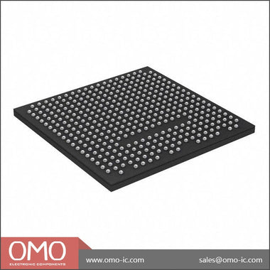
| Package | FBG676 (27x27mm) | A high-density BGA package that requires careful PCB design and layout, particularly for power delivery and high-speed signal routing. |
| Speed Grade | -1 (Commercial Temp) | Defines the maximum performance of the PL fabric and the PS. The -1 speed grade is the slowest commercial offering, balancing cost and performance. |
Reference Circuit and Component Selection
Designing a stable and reliable board around the XC7Z030-1FBG676C requires meticulous attention to several key support circuits. A failure in any of these areas can lead to system instability, boot failures, or performance degradation. The design is far more than just placing the Zynq on a PCB; it's about creating a robust ecosystem for it to operate in.
Power Delivery Network (PDN): The Zynq-7000 family has a complex power architecture with multiple voltage rails. For the XC7Z030, you must supply VCCINT (core logic), VCCAUX (auxiliary logic), VCCO (I/O banks), VCCP (PL internal supply), and rails for the PS (VCC_PSINTFP, VCC_PSAUX, etc.). A common approach is to use a Power Management IC (PMIC) specifically designed for FPGAs/SoCs, such as those from Analog Devices or Texas Instruments. These PMICs integrate multiple switching regulators, provide the correct power-up sequencing required by the Zynq (detailed in datasheet DS190), and often include voltage monitoring. Each rail requires extensive decoupling. Use a mix of capacitor values (e.g., 10µF, 1µF, 100nF, 10nF) placed as close as possible to the BGA balls to provide low impedance across a wide frequency range. The Xilinx Power Estimator (XPE) spreadsheet is an indispensable tool for calculating the current requirements for each rail based on your specific PL utilization and PS activity.
DDR Memory Interface: The PS relies heavily on external DDR3/DDR3L memory. For the FBG676 package, this is a critical high-speed interface. The layout requires 40-ohm or 50-ohm single-ended controlled impedance traces, with strict length matching for data, strobe, and clock groups. The address/command/control lines must also be length-matched. Follow the layout guidelines in Xilinx UG933 ("Zynq-7000 SoC and 7 Series FPGAs PCB Design and Pin Planning Guide") religiously. Failure to do so is a primary cause of board bring-up failures. Using a memory part from the vendor's approved list can de-risk this part of the design.
Boot and Configuration: The Zynq must be configured on power-up. The most common boot method for production systems is from an external QSPI flash memory. The boot mode is selected by strapping a few MIO (Multi-use I/O) pins to specific voltage levels using pull-up or pull-down resistors. These pins are read by the BootROM on power-on reset. The QSPI flash (e.g., a 256Mb or 512Mb part from Micron or Spansion/Cypress) connects to dedicated MIO pins on the PS. A JTAG header is also essential for initial development, programming the flash, and debugging both the PS (via ARM's CoreSight) and the PL (via Vivado Logic Analyzer).
Clocking: A stable, low-jitter clock source is non-negotiable. A typical setup includes a main system clock for the PS (e.g., 33.333 MHz or 50 MHz crystal oscillator) and potentially other dedicated oscillators for high-speed peripherals like the Ethernet PHY or the PL's data acquisition logic. The PS contains PLLs to generate the various internal clock frequencies for the ARM cores, DDR controller, and peripheral interfaces from this single input clock.
When selecting components, it's wise to consider the entire ecosystem. You can Browse Zynq-7000 Series to see different device options, but remember that the choice of PMIC, DDR memory, and clocking solution are just as critical as the Zynq device itself.
Design Pitfalls and How to Avoid Them
| Common Mistake | Symptom | Fix |
|---|---|---|
| Incorrect Power Sequencing | Device fails to boot, gets excessively hot, or is permanently damaged. JTAG chain may not be detected. | Strictly follow the power-on/power-off sequence specified in the Zynq-7000 datasheet (DS190). Use a PMIC with programmable sequencing or a dedicated sequencer IC. Verify sequence with an oscilloscope during bring-up. |
| DDR3 Layout Errors | System is unstable, crashes randomly, fails memory calibration in the First Stage Bootloader (FSBL), or won't boot at all. | Adhere to Xilinx layout guidelines (UG933). Perform signal integrity simulations (e.g., with HyperLynx) before fabrication. Ensure strict length matching, controlled impedance, and proper termination. |
| Incorrect Boot Mode Pin Strapping | The device attempts to boot from the wrong source (e.g., JTAG instead of QSPI flash), resulting in a "hung" system. | Carefully check the MIO[5:2] pin resistor pull-up/pull-down configuration against the boot mode table in the Technical Reference Manual (UG585). Ensure resistor values are appropriate and correctly placed. |
| Mismatched I/O Standards | Peripherals (ADCs, PHYs) do not communicate correctly; data is corrupted or missing. | Ensure the VCCO supply for each I/O bank matches the voltage required by the connected external device. In the Vivado design, explicitly set the I/O standard (e.g., LVCMOS33, LVDS_25) for each pin to match the hardware. |
Avoiding these pitfalls begins at the schematic capture and layout stages. One of the most common and costly mistakes is an inadequate Power Delivery Network (PDN). The dynamic current demands of a Zynq SoC can be substantial, especially when the PL fabric is heavily utilized. A weak PDN, characterized by insufficient decoupling or high-impedance power planes, will exhibit voltage droop under transient loads. This droop can cause timing violations in the digital logic, leading to intermittent, hard-to-debug failures. Always use a PCB stack-up with dedicated, solid power and ground planes. Run PI (Power Integrity) analysis using tools like those in Altium Designer or Cadence Allegro to validate the PDN design before sending the board to fabrication. Similarly, for DDR3, don't just match trace lengths; consider the entire signal path, including via and package delays, for the most critical nets.
Performance Optimization Tips
Extracting maximum performance from the XC7Z030-1FBG676C involves a holistic approach covering thermal, electrical, and logical domains.
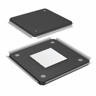
Thermal Management: The FBG676 package has a thermal pad on the underside. It is critical to design the PCB with an array of thermal vias under this pad, connecting it to internal ground planes and a large copper area on the bottom side of the board. This creates a path to dissipate heat away from the die. For a heavily utilized device in a DAQ system, a heatsink is almost always necessary. Select a heatsink and Thermal Interface Material (TIM) that provide a low thermal resistance path to the ambient air. Monitor the internal die temperature using the Zynq's built-in XADC (System Monitor) to ensure it stays within the commercial operating range (0°C to 85°C junction temperature).
EMI Reduction: A high-speed mixed-signal system is a significant source of electromagnetic interference. To mitigate EMI, start with a good PCB layer stack-up. A typical 10 or 12-layer board for a Zynq design would have signal layers sandwiched between ground planes (stripline configuration) to contain fields. Ensure an unbroken ground plane under all high-speed signals. Use ferrite beads on power supply inputs to filter high-frequency noise. Keep high-speed digital traces (like DDR3 and ADC interfaces) as far away as possible from sensitive analog circuitry.
Signal Integrity and Timing Closure: In the PL, achieving timing closure for high-frequency designs is a primary concern. Use the Vivado tool suite's capabilities to your advantage. Apply appropriate timing constraints (XDC files) from the beginning of the design cycle. For long combinatorial paths that violate timing, insert pipeline registers to break them up. For critical high-fanout nets like clocks and resets, use the dedicated global clocking resources (BUFG). Floorplanning can also help by placing related logic blocks physically close to each other on the silicon, reducing routing delays.
PS-PL Interface Optimization: The bandwidth of the AXI interconnect between the Processing System and Programmable Logic is a key performance parameter. For bulk data transfers, as in our DAQ example, always use an AXI DMA engine. Configure the DMA for large burst transactions to maximize bus efficiency. The AXI High-Performance (HP) ports on the PS provide the highest bandwidth path to DDR3 memory and should be the primary choice for data-intensive applications.
Related Components and Accessories
A successful XC7Z030-1FBG676C design depends on a well-chosen set of supporting components. For power, consider a PMIC like the Analog Devices ADP5014, which integrates four buck regulators and a controller, specifically tailored for the power sequencing and rail requirements of Xilinx 7-series devices. For DDR3L memory, reliable choices include parts from Micron's MT41K series, which are frequently validated by Xilinx. When selecting a QSPI flash for booting, a 256Mb or 512Mb device like the Micron MT25QL256ABA is a standard choice that offers sufficient space for the bootloader, bitstream, kernel, and a root filesystem.
For the Gigabit Ethernet interface required in our DAQ application, a robust external PHY is needed. The Microchip KSZ9031RNX or the Texas Instruments DP83867 are popular choices that interface with the Zynq's RGMII interface on the MIO pins. Finally, for development and debug, a JTAG programmer like the Xilinx Platform Cable USB II is essential. Once your BOM is finalized, you can Check XC7Z030-1FBG676C Inventory & Pricing to source the core of your design.
Video Demonstration
Frequently Asked Questions (XC7Z030-1FBG676C FAQ)
How do I interface high-speed ADCs to the XC7Z030's Programmable Logic?
Interfacing high-speed ADCs involves connecting their data and clock outputs to the I/O pins of the Zynq's PL. For parallel LVCMOS ADCs, you connect each data line to a separate pin. For serial LVDS ADCs, you use the dedicated ISERDES (Input SERializer/DESerializer) primitives in the PL to convert the high-speed serial stream into a wider parallel word. It is critical to use the dedicated clock-capable I/O pins (MRCC/SRCC) for the ADC clock and to correctly constrain the interface timing in your Vivado project to ensure reliable data capture at high speeds.
What is the best way to move large data sets from the PL to the PS?
The most efficient method is to use an AXI Direct Memory Access (DMA) engine. You instantiate the AXI DMA IP core in the PL fabric. This core reads data from your PL-based data source (like a FIFO buffer fed by ADCs) via an AXI-Stream interface and writes it directly into the main DDR3 memory via one of the PS's high-performance AXI ports. This offloads the ARM processor from the task of manually copying data, allowing it to focus on higher-level processing while the DMA handles the bulk transfer in the background with maximum throughput.
What power sequencing is required for the XC7Z030-1FBG676C?
The Zynq-7000 family has a strict power-on sequence to prevent latch-up and damage. According to the datasheet (DS190), the core voltage (VCCINT/VCC_PSINTFP) must ramp up first. This is followed by the auxiliary and BRAM supply (VCCAUX/VCCBRAM/VCC_PSAUX), and then the I/O voltages (VCCOs). The power-off sequence is the reverse of the power-on sequence. Using a dedicated PMIC or a hardware sequencer IC is the recommended way to guarantee this sequence is always met.
Can the ARM cores in the XC7Z030-1FBG676C run a full OS like Linux?
Yes, absolutely. The dual-core ARM Cortex-A9 processor is more than capable of running a full-featured operating system like Linux. Xilinx provides extensive support for this through its PetaLinux Tools, which offer pre-configured board support packages (BSPs), a Linux kernel, and root filesystem tailored for Zynq devices. Running Linux is highly advantageous for applications requiring networking, file systems, complex user interfaces, and a rich software development environment.
How do I debug the programmable logic and processing system simultaneously?
Xilinx provides a powerful cross-triggering mechanism for unified hardware/software debug. You can set a breakpoint in your software code running on the ARM core (using the Vitis IDE or GDB) and have it trigger a capture in the Vivado Logic Analyzer (ILA core) instantiated in the PL. Conversely, you can configure a hardware event in the PL (e.g., a specific data value on a bus) to halt the processor. This allows you to correlate software behavior with hardware events in real-time, which is invaluable for debugging complex interactions between the PS and PL.

Alan Carter
Senior Hardware Engineer & Component Specialist
Alan has over 15 years of expertise in embedded systems design, FPGA architecture, and global semiconductor supply chains. He specializes in component cross-referencing, lifecycle management, and helping OEMs navigate supply shortages.