XC7Z020-2CLG400C Design-In Guide: Why Choose It and How to Use It
Modern embedded systems frequently demand both complex, software-driven control and high-throughput, parallel data processing. Traditionally, engineers met this challenge with a two-chip solution: a microprocessor (MPU) for sequential tasks and an FPGA for parallel hardware acceleration. This approach, however, introduces significant design hurdles, including inter-chip communication latency, increased board complexity, higher power consumption, and a larger physical footprint. The Xilinx XC7Z020-2CLG400C, a member of the Zynq-7000 family, directly addresses this fundamental design pain point by integrating a powerful dual-core ARM processor system and programmable logic onto a single silicon die.

Table of Contents
The Design Challenge XC7Z020-2CLG400C Solves
The core challenge for designers of sophisticated systems—like industrial controllers, machine vision cameras, software-defined radio, and advanced driver-assistance systems (ADAS)—is the convergence of control processing and data processing. A system might need to run a full operating system like Linux to manage networking, user interfaces, and file systems, while simultaneously processing a high-speed data stream from a sensor with microsecond-level determinism. Using a separate MPU and FPGA creates a physical and architectural boundary that becomes a performance bottleneck. Data must be transferred over a parallel or serial bus (e.g., PCIe, AXI bus over FMC), which introduces latency, consumes I/O pins, and adds complexity to both hardware layout and software driver development.
The XC7Z020-2CLG400C eliminates this boundary. It is not simply an FPGA with a processor core embedded inside; it is a true System-on-Chip (SoC) where the Processing System (PS) and Programmable Logic (PL) are co-equal partners. The PS features a dual-core ARM Cortex-A9 MPCore processor, which is more than capable of running high-level operating systems and complex software stacks. The PL is based on Xilinx's 28nm Artix-7 FPGA fabric, providing a substantial amount of logic for hardware acceleration. The critical innovation is the high-bandwidth AXI interconnection fabric that links the PS and PL. This provides thousands of low-latency connections, allowing the processor to treat custom logic in the PL as if it were a memory-mapped peripheral. This tight integration allows for:
- Reduced Latency: Data can be shared between the software and hardware domains with minimal delay, which is critical for real-time control loops and signal processing pipelines.
- Increased Throughput: The wide internal bus architecture supports data transfer rates that are orders of magnitude higher than what is achievable with external chip-to-chip interfaces.
- System-Level Power Reduction: A single-chip solution eliminates the power-hungry I/O drivers needed for chip-to-chip communication, leading to a more efficient power budget.
- Smaller Form Factor: Integrating two complex devices into one saves significant PCB real estate, enabling smaller and more compact product designs.
- Design Flexibility: Engineers can partition the design optimally, placing software-intensive tasks on the ARM cores and computationally-heavy, parallelizable algorithms in the FPGA fabric. This partition can even be adjusted late in the design cycle without a hardware re-spin.
In essence, the XC7Z020-2CLG400C provides a platform to build a custom-tailored SoC for a specific application, blending the software-centric world of ARM processors with the hardware-centric world of FPGAs in a cohesive and efficient manner.
Key Specifications at a Glance
The following specifications are derived from the official Xilinx Zynq-7000 SoC (DS191) datasheet. These parameters are critical for making an informed design-in decision.
| Parameter | Value | Why It Matters |
|---|---|---|
| Processing System (PS) | Dual-Core ARM Cortex-A9 MPCore | Provides robust processing power for running operating systems (e.g., Linux), network stacks, and complex application software. The dual-core architecture supports symmetric or asymmetric multiprocessing. |
| Max CPU Frequency | 866 MHz (-2 Speed Grade) | Determines the raw performance of the software processing side. This speed grade is suitable for demanding control and application tasks. |
| Programmable Logic (PL) | 85K Logic Cells, 53,200 LUTs | This is the amount of reconfigurable logic available for custom hardware acceleration, custom peripherals, and parallel data processing. It's a substantial resource for many mid-range applications. |
| DSP Slices | 220 | These are dedicated hardware blocks for digital signal processing, ideal for accelerating filters (FIR, IIR), FFTs, and other mathematical operations common in communications and image processing. |
| Block RAM | 630 KB (5,040 Kbits) | On-chip distributed memory for buffering data within the programmable logic. Essential for creating FIFOs, data caches, and lookup tables without using external memory. |
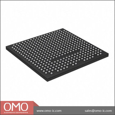
| Package | CLG400 (17x17 mm) | A 400-pin lidless chip-scale BGA. The small size is beneficial for space-constrained designs, but requires careful PCB layout and manufacturing capabilities. The lidless design requires direct thermal management. |
| User I/O | 200 | The total number of I/O pins available for custom use, split between the PS (MIO) and PL (HR/HP banks). This dictates how many external devices and interfaces can be connected. |
| Temperature Grade | Commercial (0°C to 85°C Junction) | Defines the operational thermal limits of the device. The design's thermal solution must keep the junction temperature (Tj) below 85°C under worst-case load. |
XC7Z020-2CLG400C vs Alternatives: Head-to-Head
When selecting a core processing component, it's useful to compare the Zynq-7000 SoC architecture against traditional approaches: a standalone MPU or a standalone FPGA.
| Feature | XC7Z020-2CLG400C | Standalone FPGA (e.g., Artix-7) | Standalone MPU (e.g., NXP i.MX 8M) |
|---|---|---|---|
| Core Architecture | Tightly coupled Dual ARM Cortex-A9 (PS) and FPGA fabric (PL) on one die. | Purely programmable logic fabric. Requires an external processor for software control. | Multiple ARM Cortex-A53/M4 cores. No integrated programmable logic. |
| Real-Time Determinism | Excellent. Critical loops can be implemented in the PL for nanosecond-level timing precision. | Excellent. The entire device is a hardware state machine, offering the highest level of determinism. | Limited. Real-time OS (RTOS) can help, but OS jitter makes nanosecond precision difficult. |
| System Integration | Highest. Single chip solution reduces BOM, board size, and power. | Low. Requires a separate MPU, memory, and interconnect, increasing system complexity. | Medium. Highly integrated for MPU functions, but requires an external FPGA for custom hardware. |
| Peripheral Flexibility | Very High. Standard peripherals in PS (USB, ETH, etc.) plus ability to create any custom interface in the PL. | Highest. All I/O can be configured to any standard or custom protocol. | Fixed. Limited to the hard-wired peripherals provided by the manufacturer. |
| Development Workflow | Unified (Vivado/Vitis). Hardware (HDL) and software (C/C++) development are co-dependent. | Hardware-focused (Vivado). Software development is for a separate, external processor. | Software-focused (Yocto, Android BSPs). Hardware design is limited to PCB layout. |
The decision to use the XC7Z020-2CLG400C hinges on the need for both software flexibility and hardware performance in a single, integrated package. If your application is purely a high-speed data path with minimal software control, a standalone FPGA might be a more direct solution. If your application is a media-rich user interface with standard connectivity and no need for custom hardware acceleration or real-time I/O, a standalone MPU would be more appropriate. The XC7Z020-2CLG400C excels in the middle ground, where the software and hardware are not just co-located but are fundamentally intertwined. It is the right choice when you need to run a Linux-based web server while simultaneously processing 24 parallel channels of ADC data with a custom digital filter, all on a single chip.
Recommended Application Circuit
Designing with the XC7Z020-2CLG400C is a system-level task that requires careful attention to its supporting circuitry. A minimal functional circuit must address power, configuration, clocking, and memory.
Power Distribution Network (PDN): This is the most critical aspect of a Zynq design. The device has multiple power rails for the core logic (VCCINT), auxiliary logic (VCCAUX), I/O banks (VCCO), and PS components. Each rail has specific voltage, ripple, and sequencing requirements. It is highly recommended to use a power management IC (PMIC) designed for Xilinx SoCs, such as those from Infineon or Monolithic Power Systems. These PMICs integrate multiple switching regulators and provide the correct power-up/down sequence. If designing a discrete power solution, follow the Xilinx UG933 "Zynq-7000 SoC and 7 Series FPGAs Power Methodology" guide meticulously. Extensive use of decoupling capacitors (typically 0.1uF, 1uF, 10uF) placed directly under the BGA package is mandatory for high-frequency noise suppression.
Boot and Configuration: The Zynq device boots from an on-chip BootROM, which reads a set of configuration pins (MIO[7:2]) to determine the boot device. Common options include a QSPI flash memory, an SD card, or JTAG for debugging. The design must include the chosen boot memory device connected to the appropriate MIO pins on the PS. A 16-bit or 32-bit QSPI flash is a common choice for storing the First Stage Bootloader (FSBL), the bitstream for the PL, and the application code.
DDR Memory: The PS requires an external DDR3, DDR3L, or LPDDR2 memory for program execution and data storage. The XC7Z020 supports a 16-bit or 32-bit wide memory interface. The connection between the Zynq's DDR memory controller pins and the DRAM chip is a high-speed, controlled-impedance interface. Layout is extremely critical here, demanding precise length matching and reference plane integrity.
Clocking: The PS requires a stable clock input, typically 33.333 MHz, which is used by an internal PLL to generate all other clocks for the PS subsystems. A separate clock may be provided to the PL for application-specific timing. Use a high-quality, low-jitter oscillator for the primary PS clock input.
For a comprehensive list of compatible peripherals and reference designs, you can Browse Zynq-7000 Series application notes and resources available from Xilinx and other third-party board vendors.
PCB Layout and Thermal Design Tips
The CLG400 package of the XC7Z020-2CLG400C is a 0.8mm pitch BGA, which requires an experienced PCB designer and a capable fabrication process. A minimum of 8-10 layers is typical for a successful design.
Layout Guidance:
- Fanout: Use via-in-pad (VIP) or dog-bone fanout patterns. VIP is preferred for density but increases fabrication cost. Ensure your contract manufacturer is comfortable with the chosen technology.
- Decoupling: Place decoupling capacitors on the bottom side of the PCB directly under the BGA pins they are servicing. This minimizes loop inductance. A well-planned "capacitor field" is a hallmark of a good Zynq layout.
- DDR Routing: This is arguably the most challenging part of the layout. All data (DQ), strobe (DQS), and clock traces must be length-matched within tight tolerances specified in the DDR standard. Route these signals as a group on a single layer with a solid ground reference plane.
- Power Planes: Use dedicated power planes for the main rails (VCCINT, VCC_DDR). Split planes can be used for lower-current rails, but be mindful of creating return path discontinuities for high-speed signals.
Thermal Management: The XC7Z020-2CLG400C is a lidless flip-chip package, meaning the silicon die is exposed on top. This provides an excellent thermal path but requires careful handling. The commercial grade part has a maximum junction temperature (Tj) of 85°C.
- Heatsink: For any design where both the ARM cores and a significant portion of the PL are active, a heatsink is not optional. The thermal solution must be designed to keep Tj below the 85°C limit under worst-case ambient temperature and device load.
- Thermal Interface Material (TIM): A high-quality TIM must be applied between the exposed die and the heatsink to ensure efficient heat transfer. - Airflow: Even with a heatsink, forced airflow (a fan) may be necessary depending on the calculated power dissipation, which can be estimated using the Xilinx Power Estimator (XPE) tool.
Where to Buy XC7Z020-2CLG400C
The XC7Z020-2CLG400C is a high-demand component used in a wide range of industries. As a procurement professional or design engineer, sourcing this part requires a reliable distribution partner. The part number breaks down as follows: XC (Xilinx Commercial), 7Z020 (Zynq-7000 family, device 20), -2 (speed grade), CLG400 (400-pin lidless chip-scale BGA), and C (commercial temperature range).
These devices are typically supplied in trays for high-volume manufacturing or, less commonly, in tape and reel for smaller quantities. Lead times can vary significantly based on market conditions and factory allocation. It is crucial to work with a distributor who has visibility into the global supply chain and can provide accurate lead time information and secure stock. For up-to-date availability and pricing information from a trusted global distributor, please Check XC7Z020-2CLG400C Inventory & Pricing.
Video Demonstration
Frequently Asked Questions (XC7Z020-2CLG400C FAQ)
What's the main difference between the XC7Z020 and a standard FPGA like the Artix-7?
The fundamental difference is architecture. A standard FPGA like the Artix-7 is pure programmable logic (PL); it excels at parallel hardware tasks but requires an external processor for control. The XC7Z020 is a System-on-Chip (SoC) that integrates a complete dual-core ARM Cortex-A9 processing system (PS) with FPGA fabric on the same die. This tight integration provides high-bandwidth, low-latency communication between the processor and custom hardware, which is impossible to achieve with a two-chip solution.
Do I need Xilinx's Vivado software to use the XC7Z020-2CLG400C?
Yes, the Xilinx toolchain is essential. The Vivado Design Suite is used to synthesize, place, and route your custom logic (HDL code) for the Programmable Logic (PL) portion. For the Processing System (PS), you will use the Vitis Unified Software Platform, which is integrated with Vivado. Vitis is used to develop, debug, and deploy the C/C++ application code that runs on the ARM cores, including board support packages and Linux drivers if needed.
What are the most common design mistakes when using the XC7Z020?
Three common pitfalls are power, memory, and configuration. First, an inadequate Power Distribution Network (PDN) with insufficient decoupling or incorrect power sequencing can cause stability issues that are difficult to debug. Second, incorrect PCB layout for the external DDR memory interface, such as mismatched trace lengths, will lead to memory failures. Third, improper boot mode configuration, often due to incorrect pull-up/pull-down resistors on the MIO configuration pins, can prevent the device from booting at all.
How does the XC7Z
Alan Carter
Senior Hardware Engineer & Component Specialist
Alan has over 15 years of expertise in embedded systems design, FPGA architecture, and global semiconductor supply chains. He specializes in component cross-referencing, lifecycle management, and helping OEMs navigate supply shortages.

Alan Carter
Senior Hardware Engineer & Component Specialist
Alan has over 15 years of expertise in embedded systems design, FPGA architecture, and global semiconductor supply chains. He specializes in component cross-referencing, lifecycle management, and helping OEMs navigate supply shortages.