XC7A35T-1CPG236C Datasheet, Pinout, Equivalents, and Specs
The XC7A35T-1CPG236C is a Field-Programmable Gate Array (FPGA) from the Xilinx Artix-7 family, fabricated on a 28nm HPL (High-Performance, Low-Power) process. It provides a balanced combination of logic resources, Block RAM, and DSP slices, positioning it for cost-sensitive, high-volume applications requiring significant parallel processing capabilities. This component is engineered for tasks such as industrial control, machine vision, and software-defined radio where performance-per-watt is a critical design metric.
Table of Contents
What is the XC7A35T-1CPG236C?
The XC7A35T-1CPG236C is a specific device within the Xilinx 7-series portfolio, designed to offer substantial logic density and performance while optimizing for low power consumption. The internal architecture is built around configurable logic blocks (CLBs), each containing slices with look-up tables (LUTs), flip-flops, and carry logic. This structure allows for the implementation of complex digital circuits. In addition to programmable logic, the device integrates dedicated hardware blocks such as 18Kb/36Kb Block RAMs for on-chip data storage, DSP48E1 slices for high-performance arithmetic operations, and Mixed-Mode Clock Managers (MMCMs) for precise clock synthesis and distribution. The Artix-7 family is targeted at applications that have outgrown the capabilities of microcontrollers but do not require the ultra-high performance of the Kintex or Virtex series. You can Browse Artix-7 Series to compare different devices within this family.

Pinout Configuration and Packaging
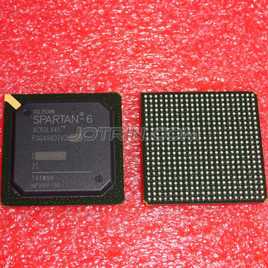
The XC7A35T-1CPG236C is supplied in a 236-pin Chip-Scale Package (CPG236), which is a 13x13 mm Ball Grid Array (BGA) with a 0.8mm pitch. This package provides a compact footprint suitable for space-constrained PCB designs. Out of the 236 pins, 106 are available as user I/O. The I/O pins are organized into High-Range (HR) banks, which support a wide range of single-ended and differential signaling standards such as LVCMOS, HSTL, and LVDS, with I/O voltages up to 3.3V. Critical pins include dedicated power (VCCINT, VCCAUX, VCCO), ground (GND), configuration pins (MODE, PROG_B, DONE, JTAG), and dedicated clock inputs (MRCC/SRCC).
Core Architectural Features
- Logic Resources: Contains 33,280 logic cells organized into 5,200 slices. Each slice includes four 6-input LUTs and eight flip-flops, providing a substantial capacity for implementing custom logic functions.
- On-Chip Memory: Features 1,800 Kb of total Block RAM, configurable as 50 individual 36 Kb blocks. Each 36 Kb block can be split into two independent 18 Kb blocks, offering flexibility for data buffering and storage.
- Digital Signal Processing (DSP): Integrates 90 DSP48E1 slices, each capable of performing a 25x18 multiply-accumulate (MACC) operation. These are essential for accelerating signal processing algorithms in applications like filtering and FFTs.
- Clock Management: Equipped with five Mixed-Mode Clock Managers (MMCMs) and one Phase-Locked Loop (PLL). These blocks provide advanced clocking capabilities, including frequency synthesis, jitter reduction, and clock deskewing.
- High-Speed Connectivity: While this specific part does not include multi-gigabit transceivers, its SelectIO interface technology supports data rates up to 1,250 Mb/s for implementing protocols like LVDS.
Specifications Parameter Table
| Specification | Technical Details |
|---|---|
| Logic Cells | 33,280 |
| Number of Slices | 5,200 |
| Total Block RAM | 1,800 Kb |
| DSP Slices | 90 |
| Maximum User I/O | 106 |
| Core Supply Voltage (VCCINT) | 1.0V (Nominal) |
| Package | CPG236 (13x13mm BGA) |
XC7A35T-1CPG236C Equivalents, Cross Reference, and Lifecycle
The XC7A35T-1CPG236C is an active production device. Finding a direct, pin-for-pin compatible equivalent from another manufacturer is not feasible due to the proprietary architecture of FPGAs. Within the Artix-7 family, other devices like the XC7A50T are available in the same CPG236 package, offering more logic resources (52,160 logic cells) for designs that require a capacity upgrade without a PCB redesign. However, the bitstream file is not compatible, and the design must be re-compiled for the new target device. When considering alternatives, it is critical to verify resource utilization (logic, BRAM, DSP) and I/O assignments. For sourcing and availability, it is recommended to Check XC7A35T-1CPG236C Inventory & Pricing to ensure component lifecycle and stock status align with project timelines.
Typical Application & Circuit Considerations
The XC7A35T-1CPG236C is well-suited for a range of embedded applications including:
- Industrial automation and motor control
- Machine vision cameras and image processing pipelines
- Software-Defined Radio (SDR) front-ends
- Medical diagnostic equipment
- Multi-axis drone and robotics controllers
Video Demonstration
Frequently Asked Questions (XC7A35T-1CPG236C FAQ)
Q: What do the suffixes in "XC7A35T-1CPG236C" denote?
A: Each part of the model number provides specific information. "-1" is the speed grade, with lower numbers indicating faster performance (e.g., -1 is faster than -L1). "C" indicates a commercial temperature range (0°C to 85°C junction temperature). "PG236" specifies the package type, which is a 236-pin plastic BGA. "C" at the end signifies the commercial temperature grade.
Q: What are the primary configuration methods for this FPGA?
A: The XC7A35T-1CPG236C supports several configuration modes, selected by the M[2:0] mode pins. The most common methods are Master SPI (x1, x2, x4), where the FPGA reads its configuration bitstream from an external SPI Flash memory, and JTAG, which is primarily used for debugging and in-system programming via a JTAG header. Slave Serial mode is also available for configuration by an external processor.
Q: How is the 1,800 Kb of Block RAM structured?
A: The total Block RAM is composed of 50 individual 36 Kb RAM blocks. Each 36 Kb block is a dual-port memory that can be configured in various ways, such as a 32Kx1, 16Kx2, 8Kx4, 4Kx9, 2Kx18, or 1Kx36 memory. Critically, each 36 Kb block can also be split into two fully independent 18 Kb dual-port RAMs, providing a total of 100 18Kb blocks if fully utilized in this mode. This offers significant flexibility for memory architecture design.
Q: What is the difference between a Logic Cell and a Slice in the Artix-7 architecture?
A: A Slice is the fundamental, physical building block of the FPGA fabric. In the Artix-7 architecture, each slice contains four 6-input LUTs, eight flip-flops, multiplexers, and carry logic. A "Logic Cell" is a more abstract marketing metric used by Xilinx to provide a rough estimate of logic capacity, generally considered to be one LUT and one flip-flop. For precise engineering and resource estimation, the number of Slices or LUTs is the more accurate and useful metric.
Q: What is the maximum I/O data rate for the XC7A35T-1CPG236C?
A: The maximum data rate depends heavily on the I/O standard being used and the speed grade of the device. For single-ended standards like LVCMOS, performance is typically in the hundreds of MHz. For high-speed differential standards like LVDS, the SelectIO interface on a -1 speed grade device can support data rates up to 1,250 Mb/s. Achieving these rates requires careful PCB design, including controlled impedance routing and proper termination.

Alan Carter
Senior Hardware Engineer & Component Specialist
Alan has over 15 years of expertise in embedded systems design, FPGA architecture, and global semiconductor supply chains. He specializes in component cross-referencing, lifecycle management, and helping OEMs navigate supply shortages.