XC6SLX9-2TQG144I Datasheet, Pinout, Equivalents, and Specs
The Xilinx XC6SLX9-2TQG144I is a Field-Programmable Gate Array (FPGA) from the well-established Spartan-6 family. It serves as a versatile logic device, solving the problem of integrating custom digital logic, I/O expansion, and co-processing in a cost-effective and power-efficient package. For hardware engineers, this device provides a flexible canvas for implementing everything from complex state machines and signal processing algorithms to simple glue logic that connects various components on a PCB. Its balance of logic resources, dedicated hardware blocks, and flexible I/O makes it a durable choice for a wide range of industrial, automotive, and consumer electronics applications.

Table of Contents
What is the XC6SLX9-2TQG144I?
The XC6SLX9-2TQG144I is a specific member of the Xilinx (now AMD) Spartan-6 FPGA family, built on a mature 45 nm low-power copper interconnect process. As an experienced hardware engineer, I see the Spartan-6 family not as the latest bleeding-edge technology, but as a reliable, well-documented, and cost-optimized solution for high-volume and long-lifecycle products. The 'LX' designation in 'XC6SLX9' signifies that it is a logic-optimized device, as opposed to the 'LXT' variants which include high-speed transceivers.
At its core, the XC6SLX9-2TQG144I provides a fabric of reconfigurable logic. The fundamental building block is the "slice," and this device contains 1,430 of them. Each slice is a rich collection of resources, primarily featuring four 6-input Look-Up Tables (LUTs) and eight flip-flops. This architecture is highly efficient; a single 6-input LUT can also be configured as two 5-input LUTs with shared inputs, allowing for very dense logic packing. In total, the device offers 9,152 logic cells, which is a metric used to estimate the equivalent ASIC gate count. This level of capacity is suitable for tasks like advanced motor control, small-scale video processing, multi-channel sensor data aggregation, and complex communication protocol implementation (e.g., CAN, SPI, I2C masters).
Beyond the general-purpose logic fabric, the XC6SLX9 integrates specialized hardware blocks that are critical for performance and efficiency. It includes 16 dedicated DSP48A1 slices. These are hardened blocks designed for digital signal processing, each containing a high-speed 18x18 multiplier, an accumulator, and pre-adder logic. Offloading DSP functions to these blocks frees up the standard logic fabric and allows the device to perform millions of multiply-accumulate operations per second, essential for filters, FFTs, and other signal processing algorithms. Additionally, the device contains 576 Kbits of Block RAM, organized in 18 Kb blocks. This fast, on-chip memory is ideal for creating FIFOs, data buffers, and storing processor instruction/data, avoiding the latency of external memory access.
The part number suffix "-2TQG144I" provides critical information: the "-2" is a standard speed grade, the "TQG144" specifies a 144-pin Thin Quad Flat Package, and the "I" denotes the industrial temperature range (-40°C to 100°C junction temperature), making it suitable for harsh environments. This combination of features makes the XC6SLX9-2TQG144I a workhorse for designs that require more flexibility than a microcontroller but do not warrant the cost or power consumption of a high-end FPGA or an ASIC.
Pinout Configuration and Packaging
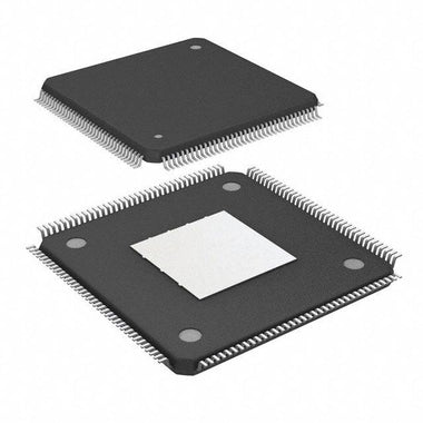
The XC6SLX9-2TQG144I is supplied in a TQG144 package, which stands for a 144-pin Thin Quad Flat Package with an exposed ground pad. From a practical engineering standpoint, this package is a significant feature. Unlike BGA (Ball Grid Array) packages, TQFP packages have leads extending from the sides, making them visually inspectable and easier to hand-solder during prototyping or rework. This significantly lowers the barrier to entry for smaller companies or for initial board bring-up, as it doesn't require expensive X-ray inspection equipment.
The 144 pins are allocated to several functions critical for system integration:
- User I/O Pins: The TQG144 package for the XC6SLX9 provides up to 102 user-configurable I/O pins. These pins are organized into I/O banks, each with its own VCCO power supply pin. This allows different banks to operate at different voltage standards (e.g., one bank at 3.3V LVCMOS for an Ethernet PHY and another at 1.8V for an ADC), enabling seamless integration in a mixed-voltage system.
-
Power Supply Pins: A robust Power Delivery Network (PDN) is crucial. The device requires three main supplies:
- VCCINT: The core voltage, nominally 1.2V, which powers the internal logic fabric, Block RAM, and DSP slices. This is the main power consumer.
- VCCAUX: The auxiliary supply, nominally 2.5V, which powers resources like the JTAG interface, clock management tiles, and some I/O internal logic.
- VCCO: The I/O bank voltage, which can range from 1.2V to 3.3V depending on the I/O standard being used. Each I/O bank has its own VCCO pins.
- Configuration Pins: These pins are used to load the configuration bitstream into the FPGA upon power-up. Key pins include M0, M1, and M2 for selecting the configuration mode (e.g., Master SPI, Slave Serial), CCLK (configuration clock), and DONE, which signals a successful configuration.
- JTAG Pins: The standard IEEE 1149.1 Test Access Port pins (TCK, TMS, TDI, TDO) are present for programming, debugging (using tools like ChipScope Pro), and boundary-scan testing.
- Dedicated Clock Inputs: The device has dedicated global clock input pins (GCLK) that are routed onto a high-speed, low-skew global clock network to ensure proper timing across the entire chip.
The exposed thermal pad on the underside of the package is not just for grounding; it is essential for thermal management. It must be soldered to a corresponding copper area on the PCB, often with thermal vias, to effectively dissipate heat from the die to the board's ground plane.
Core Architectural Features
- Advanced 6-Input LUT Fabric: The core of the Spartan-6 logic is its 6-input Look-Up Table (LUT) architecture. This provides a significant advantage in logic density, as each LUT can implement any 6-input Boolean function. Critically, it can also be fractured into two 5-input LUTs with shared inputs, allowing the synthesis tools to pack logic more efficiently compared to older 4-input LUT architectures. Each LUT is paired with flip-flops within the slice, enabling the creation of complex registered logic with minimal routing delay.
- Integrated DSP48A1 Slices: The device includes 16 dedicated DSP48A1 slices. These are not soft logic but hardened, power-efficient blocks designed for high-performance arithmetic. Each slice features an 18x18 two's complement multiplier, a 48-bit accumulator, and a pre-adder. This makes the XC6SLX9 highly capable for applications requiring filtering, correlation, or other DSP functions, achieving performance that would be impossible or grossly inefficient to implement in the general logic fabric.
- Flexible Clock Management Tiles (CMTs): Timing is everything in digital design. The XC6SLX9 features two CMTs, each containing two Digital Clock Managers (DCMs) and one Phase-Locked Loop (PLL). These blocks provide sophisticated clocking capabilities, including frequency synthesis (multiplying/dividing clocks), clock de-skew to eliminate internal clock path delay differences, and jitter filtering for cleaning up noisy clock sources. This robust clocking infrastructure is essential for building reliable, high-speed systems.
- High-Performance SelectIO Technology: The device's I/O blocks support a vast array of signaling standards, including single-ended standards like LVCMOS and LVTTL at various voltages (3.3V, 2.5V, 1.8V, etc.) and differential standards like LVDS and TMDS. This flexibility allows the FPGA to directly interface with a wide variety of other components without requiring external level-shifting or translation logic. The I/O blocks also contain advanced features like individually controllable pull-up/pull-down resistors and the IODELAY2 primitive for fine-grained, per-bit input delay tuning.
- Comprehensive Power-Saving Modes: Built on a 45 nm process, the Spartan-6 family was designed with power efficiency in mind. The XC6SLX9 supports multiple power-saving modes. This includes a low-power Suspend mode that retains the FPGA's configuration and internal state while powering down most of the internal logic, and an even lower-power Hibernate mode where the device is almost completely powered off but can be quickly woken up by an external event. These features are critical for battery-powered or thermally constrained applications.
Specifications Parameter Table
| Specification | Technical Details |
|---|---|
| Logic Cells | 9,152 |
| Number of Slices | 1,430 |
| Number of 6-input LUTs | 5,720 |
| Total Block RAM | 576 Kbits (32 blocks of 18 Kb each) |
| DSP48A1 Slices | 16 |
| Core Voltage (VCCINT) | 1.2V Nominal (1.14V to 1.26V) |
| Maximum User I/O (TQG144 Package) | 102 |
| Operating Junction Temperature (Industrial Grade) | -40°C to 100°C |
XC6SLX9-2TQG144I Equivalents, Cross Reference & Lifecycle
The XC6SLX9-2TQG144I is a mature product. While it is still in production and available for existing designs, it is generally not recommended for new designs (NRND) by AMD/Xilinx, who encourage migration to newer families like the Artix-7. However, its long history means it has a stable supply chain for companies with long-life products. You can Check XC6SLX9-2TQG144I Inventory & Pricing for current availability.
Finding a direct, 100% drop-in replacement for an FPGA is nearly impossible. The "personality" of an FPGA is defined by its bitstream, which is compiled specifically for its architecture. Therefore, "equivalents" must be considered in terms of function and resources, not as simple drop-in parts.
- Within the Spartan-6 Family: The most straightforward substitution is within the same family. If a design requires higher performance, the XC6SLX9-3TQG144I (the -3 speed grade) is pin-compatible and offers faster timing, but requires re-running timing analysis. If more logic is needed, the XC6SLX16-2TQG144I offers more resources (15,822 logic cells) in the same package, but this is a different die and requires a complete re-compile and re-verification of the design.
- Functional Equivalents for New Designs: For new projects, a hardware engineer would look at modern alternatives. A comparable device from the Intel/Altera portfolio would be a member of the Cyclone IV or Cyclone V family. For a migration path within the AMD/Xilinx ecosystem, a device like the Artix-7 XC7A15T in a similar package would be a common choice. It offers significantly more performance, lower power, and is supported by the modern Vivado Design Suite. However, this constitutes a complete redesign, involving new software tools, new IP cores, and a new PCB layout.
Typical Applications & Circuit Considerations
The XC6SLX9-2TQG144I's blend of low cost, sufficient logic density, and dedicated hardware blocks makes it a versatile component in many systems. Its industrial temperature rating further expands its utility into non-benign environments.
Typical Applications Include:
- Industrial Automation: Implementing real-time motor control loops (PWM generation, encoder feedback processing), interfacing with multiple industrial sensors, and acting as a flexible backplane controller.
- Video and Imaging: While not a high-end video processor, it is perfectly capable of simple video tasks like format conversion (DVI/HDMI to LVDS), image sensor interfacing, on-the-fly color space conversion, and overlaying graphics on a video stream.
- Communications and Networking: Acting as a "glue logic" powerhouse to bridge different communication standards, implementing custom bus protocols, or creating a multi-port UART/SPI/I2C expander for a host processor.
- Legacy System Emulation: The reconfigurable nature of FPGAs makes them ideal for recreating the behavior of obsolete ASICs or processors, allowing for the modernization of legacy systems without changing the software.
Circuit Design and PCB Layout Considerations:
Successfully integrating the XC6SLX9-2TQG144I requires careful attention to the surrounding circuitry. The power delivery network (PDN) is paramount. The 1.2V core supply (VCCINT) can have high-frequency current demands, requiring a tight layout with multiple low-ESR ceramic decoupling capacitors placed as close as possible to the device's power pins. A mix of capacitor values (e.g., 10µF, 1µF, 100nF, 10nF) is recommended to provide low impedance across a wide frequency range. The VCCAUX and VCCO rails have similar requirements, though typically less stringent than the core.
Power sequencing is also a consideration detailed in the datasheet; typically, VCCINT should ramp up first or at the same time as VCCAUX and VCCO. Configuration is another key area. The FPGA is SRAM-based and loses its configuration on power-down. Therefore, an external non-volatile memory, typically a low-cost SPI flash chip, is required to store the bitstream. The FPGA is configured to act as a Master, clocking the data out of the SPI flash into itself upon power-up.
Finally, while the TQFP package is more forgiving than a BGA, good high-speed design practices are still necessary. Keep clock traces short and properly terminated, ensure clean return paths for signals on adjacent ground planes, and pay attention to the routing of differential pairs if used. The entire Browse Spartan-6 Series offers a range of options, but the fundamental design principles remain consistent.
Video Demonstration
Frequently Asked Questions (XC6SLX9-2TQG144I FAQ)
What is the difference between the XC6SLX9 and the XC6SLX16?
The primary difference is the amount of internal logic resources. The XC6SLX9-2TQG144I has 9,152 logic cells, 1,430 slices, and 576 Kbits of Block RAM. The XC6SLX16, in the same package, offers a significant increase to 14,579 logic cells, 2,278 slices, and 576 Kbits of Block RAM. Choosing between them is a matter of design requirements; if your design fits within the XC6SLX9, it is the more cost-effective choice. If you need more logic or anticipate future feature additions, the XC6SLX16 provides that extra capacity.
What software is used to program the XC6SLX9-2TQG144I?
The Spartan-6 family, including the XC6SLX9, is supported by the Xilinx ISE Design Suite. The last version to fully support Spartan-6 is ISE 14.7. It is important to note that this family is NOT supported by the modern Xilinx Vivado Design Suite, which is used for 7-series devices and newer. This is a critical distinction for development environment setup and long-term project maintenance.
Is the XC6SLX9-2TQG144I a 5V tolerant device?
No, it is not. The I/O pins are not 5V tolerant. According to the official datasheet, the absolute maximum voltage on a user I/O pin is 4.1V, and the recommended operating conditions top out at 3.3V for high-range I/O standards like LVCMOS33. Applying 5V directly to an I/O pin will damage the device. If interfacing with 5V logic is required, you must use external level-shifting circuitry or a 5V-tolerant buffer.
What kind of external memory is needed for configuration?
The XC6SLX9 is an SRAM-based FPGA, meaning it needs to be configured from an external source at every power-on. The most common method is using an external SPI flash memory chip. The FPGA is set to "Master SPI" configuration mode, where it generates the clock and reads the bitstream from the flash. A 16 Mbit SPI flash is typically more than sufficient for the XC6SLX9's bitstream, which is approximately 2.6 Mbits in size.
What does the "-2TQG144I" suffix mean?
This suffix is a breakdown of the device's specific variant. "-2" indicates the speed grade; -2 is a standard commercial/industrial speed, while -3 would be a faster (and more expensive) grade. "TQG" refers to the package type: Thin Quad Flat Package. "144" is the pin count. Finally, "I" specifies the operating temperature range, which is Industrial grade (-40°C to 100°C junction temperature), as opposed to "C" for Commercial (0°C to 85°C).