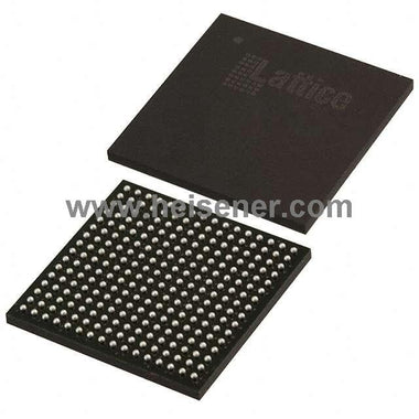
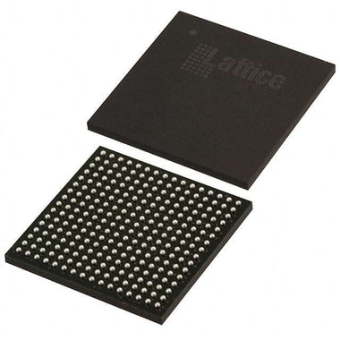
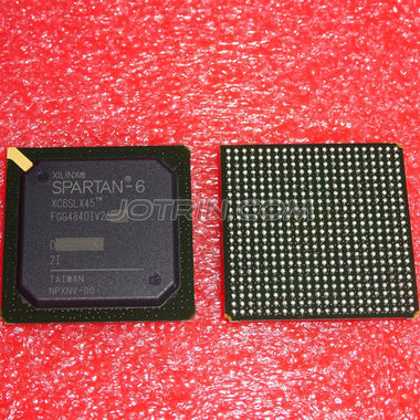
The XC6SLX9-2TQG144I is a field-programmable gate array (FPGA) from the Xilinx (now AMD) Spartan-6 family, representing a mature and cost-effective solution for a wide range of digital logic applications. It provides a flexible platform for implementing custom digital circuits, bridging interfaces, and accelerating algorithms in hardware. This device is particularly well-suited for designs requiring a balance of logic capacity, performance, and low power consumption, making it a workhorse in industrial, communications, and consumer electronics for over a decade.
Table of Contents
What is the XC6SLX9-2TQG144I?
The XC6SLX9-2TQG144I is a specific member of the Xilinx Spartan-6 LX series, optimized for logic-intensive designs. Built on a proven 45 nm process technology, it offers a significant density and performance uplift compared to its predecessors while managing power consumption effectively. At its core, the device is a sea of reconfigurable logic blocks surrounded by programmable I/O and supported by dedicated, hardened functional blocks.
The fundamental building block of the Spartan-6 architecture is the slice. The XC6SLX9 contains 1,430 slices. Unlike previous architectures, Spartan-6 utilizes a more advanced 6-input look-up table (LUT) structure. Each slice contains four LUTs and eight flip-flops/latches. These 6-input LUTs are highly flexible and can be configured as one 6-input function, two 5-input functions with shared inputs, or even as distributed RAM or shift registers (SRL16/SRL32). This flexibility allows the synthesis tools to pack logic more efficiently, leading to better device utilization and potentially higher performance compared to older 4-input LUT architectures.
Beyond the general-purpose logic fabric, the XC6SLX9 integrates several critical hard IP blocks to offload common, resource-intensive tasks. It includes 576 Kb of true dual-port Block RAM, organized in 18 Kb blocks. This memory is essential for creating data buffers, FIFOs, and storing processor instruction/data memory. For computationally intensive applications, the device features 16 dedicated DSP48A1 slices. Each DSP slice contains a high-speed 18x18 multiplier, an adder, and an accumulator, making it ideal for implementing digital filters (FIR, IIR), Fast Fourier Transforms (FFTs), and other signal processing algorithms without consuming the general-purpose logic fabric.
Clocking is managed by two Clock Management Tiles (CMTs). Each CMT includes two Digital Clock Managers (DCMs) and one Phase-Locked Loop (PLL). These blocks are crucial for robust clock network design, allowing for clock synthesis (multiplication/division), phase shifting, clock deskew, and jitter reduction. Proper use of the CMTs is fundamental to achieving timing closure in any high-speed design.
The "-2" in the part number denotes its speed grade, which represents a standard performance level. The "TQG144I" suffix specifies the packaging: a 144-pin Thin Quad Flat Pack (TQFP), which is leaded and relatively easy to solder, making it suitable for prototyping and volume production. The "I" signifies the industrial temperature range, guaranteeing operation from -40°C to 100°C junction temperature, a requirement for non-benign operating environments.
Pinout Configuration and Packaging
The XC6SLX9-2TQG144I is offered in the TQG144 package, a 144-pin Thin Quad Flat Pack. This package is a popular choice due to its balance of pin density and ease of assembly, as it does not require the complex BGA rework equipment. Of the 144 pins, 102 are available as user I/O, providing ample connectivity for most target applications.
The pins are not just generic I/O; they are organized into banks, each with its own VCCO power supply pin. This allows different I/O banks to operate at different voltage standards (e.g., 3.3V LVCMOS on one bank, 2.5V on another), facilitating seamless integration in mixed-voltage systems. It is critical to power all VCCO pins, even for unused banks, according to the datasheet recommendations.
Key pin categories include:
- User I/O: The 102 general-purpose I/O pins that can be configured for various standards like LVCMOS, HSTL, and SSTL.
- Power Pins: Multiple pins for core voltage (VCCINT = 1.2V), auxiliary voltage (VCCAUX), and I/O bank voltages (VCCO). A robust power delivery network with proper decoupling is non-negotiable for stable operation.
- Ground Pins (GND): Numerous ground pins are provided and must all be connected to a solid ground plane to ensure signal integrity and minimize noise.
- Configuration Pins: These pins control how the FPGA loads its configuration data upon power-up. Key pins include PROG_B (to initiate reconfiguration), DONE (indicates successful configuration), CCLK (for serial configuration modes), and the mode pins (M0, M1, M2) which select the configuration source (e.g., JTAG, SPI Flash).
- JTAG Pins: TMS, TCK, TDI, and TDO form the JTAG Test Access Port, used for programming, debugging (with tools like ChipScope Pro), and boundary-scan testing. These pins are essential for development and board-level test.
- Global Clock Pins: Dedicated GCLK pins are connected to the internal global clock network, providing low-skew distribution paths for high-fanout clock signals. Driving primary system clocks through these inputs is best practice.
Engineers must consult the official Xilinx documentation for the exact pinout diagram for the TQG144 package, as pin functions can be multiplexed. Careful pin planning during the schematic design phase is crucial to ensure signal integrity, meet timing requirements, and avoid routing congestion.
Core Architectural Features
- Advanced Logic Fabric: The device is built around 9,152 logic cells, arranged in 1,430 slices. Each slice contains four 6-input LUTs and eight flip-flops, providing a highly efficient structure for implementing complex combinatorial and sequential logic. The 6-input LUTs can be fractured into two 5-input LUTs, maximizing logic density.
- Dedicated DSP Slices: Includes 16 high-performance DSP48A1 slices. Each slice integrates an 18x18 two's complement multiplier, a 48-bit accumulator, and a pre-adder, capable of running at high clock frequencies. These are invaluable for implementing DSP functions like MAC (Multiply-Accumulate) operations in hardware, freeing up logic fabric.
- Block RAM and Memory Support: Features 576 Kb of true dual-port Block RAM, configurable in 18 Kb blocks. This memory is ideal for on-chip data buffering, implementing FIFOs, or serving as memory for soft-core processors. Additionally, the Spartan-6 family includes a hard Memory Controller Block (MCB) for interfacing with external DDR, DDR2, LPDDR, and DDR3 memory (availability dependent on package/pinout).
- Robust Clock Management: Equipped with two Clock Management Tiles (CMTs), each containing two DCMs and one PLL. These blocks provide sophisticated clocking capabilities, including frequency synthesis, clock de-skew for board-level timing, phase shifting, and jitter filtering, which are essential for stable operation in high-speed systems.
- Flexible I/O and Configuration: Offers up to 102 user I/O pins in the TQG144 package, supporting a wide array of I/O standards. The device supports multiple configuration modes, including Master/Slave SPI from an external flash memory, and JTAG for development and debugging. The power-on-reset and configuration sequence is robust and well-documented.
Specifications Parameter Table
| Specification | Technical Details |
|---|---|
| Part Number | XC6SLX9-2TQG144I |
| FPGA Family | Spartan-6 LX |
| Logic Cells | 9,152 |
| Number of Slices | 1,430 |
| Total Block RAM | 576 Kbits (32 blocks of 18 Kb) |
| DSP48A1 Slices | 16 |
| Maximum User I/O | 102 |
| Core Voltage (VCCINT) | 1.2V (Nominal) |
| Package | 144-pin Thin Quad Flat Pack (TQG144) |
| Speed Grade | -2 (Standard Performance) |
| Temperature Grade | Industrial (-40°C to 100°C Junction Temperature) |
XC6SLX9-2TQG144I Equivalents, Cross Reference & Lifecycle
The XC6SLX9-2TQG144I is part of the mature Spartan-6 family, which is now considered a legacy product by AMD/Xilinx, though it remains in production to support existing designs. For new designs, engineers are strongly encouraged to use newer families like Spartan-7 or Artix-7, which offer better performance, lower power, and are supported by the modern Vivado Design Suite.
Finding a direct, 100% drop-in equivalent for an FPGA is extremely difficult. However, within the Spartan-6 family, some level of migration is possible:
- XC6SLX16-2TQG144I: This is a larger device in the same family and package. If a board was designed with future expansion in mind, it might be possible to use this part if more logic resources are needed. However, this is not a direct cross; the bitstream file is different, and the design must be re-compiled for the new target device.
- Different Speed/Temp Grades: A part like XC6SLX9-3TQG144I (faster speed grade) or XC6SLX9-2TQG144C (commercial temperature grade) might be considered. Substituting a faster speed grade is usually safe, but the design must be re-verified through static timing analysis. Substituting a commercial grade part for an industrial one is only acceptable if the application's environmental requirements permit it.
It is crucial to understand that FPGAs are not like simple logic gates; they are complex systems. Any substitution requires a full design re-synthesis, re-implementation, and re-verification of timing constraints. For procurement, it's essential to manage the lifecycle of this component. While still available, supply can fluctuate. Verifying stock and lead times is a critical step in production planning. Check XC6SLX9-2TQG144I Inventory & Pricing to get the most current availability information.
Typical Applications & Circuit Considerations
The XC6SLX9-2TQG144I has found a home in a vast number of applications where cost-effective, flexible digital logic is required. Its combination of logic, DSP, and memory resources makes it a versatile choice. Common applications include:
- Industrial Automation: Implementing custom motor control loops, interfacing with various sensors, and creating custom communication bus controllers (e.g., CAN, EtherCAT slave).
- Machine Vision: Performing real-time image pre-processing tasks like color space conversion, filtering, and edge detection before data is sent to a host processor.
- Protocol Bridging: Acting as a "glue logic" powerhouse to connect disparate interfaces, such as bridging a legacy parallel bus to a modern SPI or I2C interface, or creating a custom UART with a deep FIFO.
- Consumer Electronics: Driving small displays, audio processing, and managing system control functions in devices where an ASIC is not cost-effective.
- Software Defined Radio (SDR): Performing digital down-conversion (DDC) or digital up-conversion (DUC) and filtering in the digital domain.
When designing a board with the XC6SLX9, several circuit considerations are paramount. The power delivery network (PDN) is arguably the most critical. The device requires multiple voltage rails: VCCINT (1.2V) for the core, VCCAUX for auxiliary internal logic, and one or more VCCO rails for the I/O banks. Each power rail must be properly decoupled with a combination of bulk capacitance (e.g., 10-100µF) and high-frequency ceramic capacitors (e.g., 0.1µF, 0.01µF) placed as close as possible to every power pin. Referencing the UG393, Spartan-6 FPGA PCB Design and Pin Planning Guide, is mandatory.
Power sequencing is also important. While Spartan-6 is generally tolerant, the recommended power-on sequence is VCCINT, then VCCAUX, then VCCO. This ensures the internal logic is stable before the I/Os become active. Configuration is another key area. A common setup is to use a small, low-cost SPI flash memory to store the FPGA's configuration bitstream. The FPGA is set to Master SPI mode and automatically reads its configuration from the flash upon power-up. Ensure the SPI flash is compatible and that the connections between the FPGA and flash (CCLK, MOSI, MISO, CS) are short and clean.
For any high-speed I/O, PCB layout must follow controlled impedance rules to maintain signal integrity. This involves careful track width and spacing calculations based on the PCB stack-up. For a comprehensive look at what's possible with this architecture, you can Browse Spartan-6 Series to see the full range of devices and their capabilities.
Video Demonstration
Frequently Asked Questions (XC6SLX9-2TQG144I FAQ)
What software is used to program the XC6SLX9-2TQG144I?
The XC6SLX9-2TQG144I is exclusively supported by the Xilinx ISE Design Suite, typically version 14.7, which was the final release. It is not supported by the modern Xilinx Vivado Design Suite, which is used for 7-series and newer devices. Engineers working with Spartan-6 must use ISE for all design stages, including HDL synthesis, place-and-route, timing analysis, and bitstream generation.
What is the difference between the -2 and -3 speed grades?
The number after the device name, like the "-2" in XC6SLX9-2TQG144I, indicates the speed grade. A higher number signifies a faster part. For example, a -3 speed grade part has tighter timing specifications and can generally be clocked faster than a -2 part. A -2 speed grade is considered standard performance, while a -3 is a high-performance grade. When selecting a speed grade, you must ensure your design can meet timing closure with the chosen part.
What do the letters in "TQG144I" mean?
This code defines the package and device properties. "TQ" stands for Thin Quad Flat Pack package type. "G" indicates that the package is RoHS compliant (lead-free). "144" is the pin count. Finally, the "I" at the end specifies the industrial temperature range, which guarantees operation with a junction temperature between -40°C and 100°C, making it suitable for harsh environments.
Can this FPGA run a soft-core processor?
Yes, absolutely. The XC6SLX9 has sufficient logic resources and Block RAM to instantiate a soft-core processor like the Xilinx MicroBlaze. This allows you to create a full System-on-Chip (SoC) design, combining custom hardware accelerators in the FPGA fabric with software running on the processor. This is a common use case for handling complex control, communication protocols, and user interfaces.
What are the main power supply requirements?
The Spartan-6 family requires a multi-rail power supply. The three primary rails are VCCINT (1.2V nominal) for the internal core logic, VCCAUX (2.5V nominal) for auxiliary logic like JTAG and configuration, and VCCO for the user I/O banks. The VCCO voltage is flexible (e.g., 1.8V, 2.5V, 3.3V) and must match the I/O standard you intend to use for that bank. Each rail requires careful decoupling with capacitors placed close to the device pins.

Alan Carter
Senior Hardware Engineer & Component Specialist
Alan has over 15 years of expertise in embedded systems design, FPGA architecture, and global semiconductor supply chains. He specializes in component cross-referencing, lifecycle management, and helping OEMs navigate supply shortages.