EP4CGX150DF27C7N Datasheet, Pinout, Equivalents, and Specs
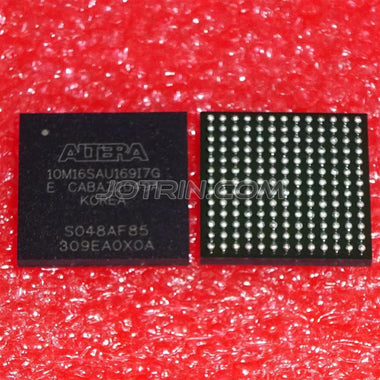
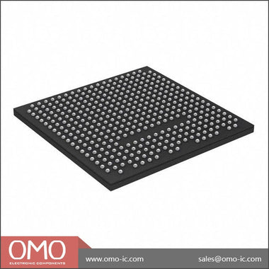
The EP4CGX150DF27C7N is a high-density FPGA from Intel's (formerly Altera) Cyclone IV GX family, built on a 60nm process node. Featuring 149,760 logic elements, eight integrated 3.125 Gbps transceivers, and 6,635,520 embedded memory bits, it targets cost-sensitive applications requiring serial connectivity such as PCI Express Gen1, serial RapidIO, and CPRI/OBSAI base-station interfaces. The device ships in a 672-ball FBGA package (27 × 27 mm) at commercial temperature grade (0 °C to 85 °C) with a –7 speed grade.
What Is the EP4CGX150DF27C7N?
The EP4CGX150DF27C7N belongs to the Cyclone IV GX sub-family — Intel's lowest-cost FPGA line that integrates full-duplex transceivers. The "GX" designation specifically indicates the presence of high-speed serial I/O blocks, distinguishing it from the Cyclone IV E variants that lack transceivers. Internally the device organizes 149,760 logic elements into 9,360 Logic Array Blocks (LABs), each containing 16 adaptive logic modules (ALMs). Embedded memory is distributed across 720 M9K blocks (each providing 9,216 bits), totaling 6,635,520 bits of on-chip SRAM configurable as single-port RAM, dual-port RAM, FIFO buffers, or ROM.
On the DSP front, 360 embedded 18 × 18 multipliers enable efficient implementation of multiply-accumulate (MAC) operations for signal-processing datapaths. Clock management relies on eight PLLs — four general-purpose and four dedicated — delivering frequency synthesis, clock multiplication and division, and phase-shift capabilities across up to 10 independent I/O banks. The eight transceivers support data rates from 600 Mbps to 3.125 Gbps, with a built-in PCI Express hard IP block that can configure x1, x2, or x4 endpoint links at Gen1 speeds.

Pinout Configuration and Packaging
The EP4CGX150DF27C7N is housed in a 672-ball FineLine BGA (FBGA) package designated F27 (27 × 27 mm body, 1.0 mm ball pitch). Of the 672 balls, 393 are available as user I/O, distributed across 10 I/O banks plus one dedicated configuration bank. Each I/O bank supports independent VCCIO supply rails, enabling mixed-voltage interfacing (1.2 V, 1.5 V, 1.8 V, 2.5 V, and 3.3 V) within a single device.
Critical power pins include VCCINT (1.2 V core), VCCIO (per-bank selectable), and VCCA / VCCD (analog and digital PLL supply at 2.5 V and 1.2 V respectively). Transceiver reference clock inputs reside on dedicated differential pairs (REFCLK0/1) and should be routed with impedance-controlled differential traces. The configuration bank supports multiple modes — Active Serial (AS), Passive Serial (PS), Fast Passive Parallel (FPP), and JTAG — via the MSEL[3:0] pin strapping.

Specifications Parameter Table
| Specification | Technical Details |
|---|---|
| Device Family | Cyclone IV GX (Intel / Altera) |
| Logic Elements (LEs) | 149,760 |
| Logic Array Blocks (LABs) | 9,360 |
| Embedded Memory | 6,635,520 bits (720 × M9K blocks) |
| Embedded Multipliers | 360 (18 × 18-bit) |
| PLLs | 8 total (4 general-purpose + 4 dedicated) |
| Transceivers | 8 full-duplex channels, 600 Mbps – 3.125 Gbps |
| User I/O Pins | 393 |
| Package | 672-FBGA, 27 × 27 mm, 1.0 mm pitch |
| Process Node | 60 nm TSMC |
| Core Voltage | 1.2 V (VCCINT) |
| Speed Grade | –7 (Commercial, 0 °C to 85 °C) |
| I/O Standards | LVDS, SSTL, HSTL, LVCMOS, LVTTL, PCI, PCI-X |
| PCIe Hard IP | Gen1 x1 / x2 / x4 endpoint |
| Configuration Modes | AS, PS, FPP, JTAG |
Typical Applications and Circuit Considerations
The EP4CGX150DF27C7N is widely deployed in designs that require moderate logic density combined with multi-gigabit serial links at the lowest possible BOM cost. Typical system-level applications include:
- Wireless Base-Station Interface Cards: CPRI/OBSAI front-haul links between radio heads and baseband units leverage the 3.125 Gbps transceivers while the embedded multipliers handle digital up/down-conversion filtering.
- Industrial Vision and Video: Camera Link, SDI, and proprietary high-speed serial video pipelines use the transceiver channels for data ingestion, with M9K blocks serving as line buffers.
- PCI Express Endpoint Controllers: The Gen1 hard IP block allows rapid bring-up of x1/x4 PCIe endpoint adapters for data-acquisition boards, NIC offload engines, or test & measurement instruments.
- Networking and Switching: Small-form-factor switches and routers use multiple transceiver channels for SGMII or GbE PHY interfaces with low-latency packet processing in fabric logic.
From a circuit-design standpoint, Intel recommends separate filtered 1.2 V supplies for VCCINT and VCCD, with ferrite-bead isolation between the core and PLL digital domains. Each transceiver quad requires its own 2.5 V VCCA_L rail filtered by a dedicated LC network. Decoupling capacitors (100 nF MLCC per power pin, plus 10 µF bulk per rail) should be placed as close to the BGA pads as possible on the inner PCB layers. High-speed differential pairs for transceivers demand 100 Ω differential impedance with length-matched routing and AC-coupling capacitors (100 nF, 0402) at the transmitter output.

Video: Getting Started with Altera Cyclone IV FPGA and Quartus II
Equivalents, Cross-Reference, and Lifecycle
The EP4CGX150DF27C7N carries an Active lifecycle status as of 2026, with no Product Discontinuation Notice (PDN) issued. Intel continues to manufacture the Cyclone IV GX family through its mature-node foundry agreements. However, lead times have periodically extended beyond 30 weeks during supply-chain disruptions, making cross-referencing critical for procurement teams.
Within the Cyclone IV GX family, the closest pin-compatible variants in the same F27 package are:
- EP4CGX150DF27C8N — identical die, –8 (slower) speed grade. Drop-in replacement when timing margins permit.
- EP4CGX150DF27I7N — industrial-temperature variant (–40 °C to 100 °C), functionally identical, same pinout.
Cross-family migration paths:
- Intel Cyclone V GX (5CGXFC7D6F27C7N): 28 nm successor with higher logic density (150K LEs) and 6.144 Gbps transceivers. Not pin-compatible but shares a similar architecture, easing RTL migration. Offers lower static power.
- Lattice ECP5-5G (LFE5UM5G-85F-8BG381C): 85K LUTs with 5 Gbps SERDES in a smaller BGA. Competitive on price for designs that do not require the full 150K LE density.
For engineers evaluating alternative Intel FPGAs, see also our technical guides on the EP4CE6E22C8N Cyclone IV E, the Xilinx XC7K325T Kintex-7, and the Xilinx XC7A200T Artix-7.
Market Availability and Pricing Trends
The EP4CGX150DF27C7N occupies the high end of Intel's cost-optimized FPGA portfolio, with unit pricing typically in the $80–$150 range depending on volume and distributor. Market availability has stabilized following the 2021–2023 semiconductor shortage cycle, though spot-market premiums can still appear during demand spikes in telecom and industrial sectors.
To check real-time stock, pricing, or to request a quote for the EP4CGX150DF27C7N and its verified alternatives, upload your BOM to WWDParts for fast processing.
Frequently Asked Questions (FAQ)
What is the maximum transceiver data rate of the EP4CGX150DF27C7N?
The EP4CGX150DF27C7N supports eight full-duplex transceiver channels with data rates ranging from 600 Mbps to 3.125 Gbps. These transceivers include both PMA (Physical Media Attachment) and PCS (Physical Coding Sublayer) blocks and support protocols such as PCI Express Gen1, Gigabit Ethernet (SGMII), CPRI, and OBSAI.
What package does the EP4CGX150DF27C7N use and how many user I/O pins are available?
The device is packaged in a 672-ball FineLine BGA (FBGA) with a 27 × 27 mm body and 1.0 mm ball pitch. It provides 393 user I/O pins distributed across 10 I/O banks, each supporting independent VCCIO voltage levels from 1.2 V to 3.3 V.
Is the EP4CGX150DF27C7N pin-compatible with the industrial-grade EP4CGX150DF27I7N?
Yes. The EP4CGX150DF27I7N is the industrial-temperature variant (–40 °C to 100 °C) of the same silicon die in the same 672-FBGA F27 package. It is fully pin-compatible and functionally identical, making it a direct drop-in replacement for designs that require an extended operating temperature range.
What design software is required to develop with the EP4CGX150DF27C7N?
The EP4CGX150DF27C7N is supported by Intel Quartus Prime Lite Edition (free, no license required) and Quartus Prime Standard Edition. Cyclone IV GX devices require Quartus version 13.0 SP1 or later. The design flow supports Verilog, VHDL, and schematic entry, along with the Platform Designer (formerly Qsys) system integration tool.
How much on-chip memory does the EP4CGX150DF27C7N provide?
The device contains 6,635,520 bits (approximately 6.3 Mbit) of embedded SRAM organized as 720 M9K memory blocks. Each M9K block offers 9,216 bits and can be configured as single-port RAM, simple or true dual-port RAM, ROM, or FIFO buffers with independent read/write clocks.
What power supply voltages are needed for the EP4CGX150DF27C7N?
The core logic (VCCINT) requires 1.2 V. Each I/O bank has an independent VCCIO rail selectable from 1.2 V, 1.5 V, 1.8 V, 2.5 V, or 3.3 V. The PLL analog supply (VCCA) requires 2.5 V, while the PLL digital supply (VCCD) uses 1.2 V. Transceiver analog supply (VCCA_L) is 2.5 V per quad. Intel recommends ferrite-bead isolation between VCCINT and VCCD domains.

Alan Carter
Senior Hardware Engineer & Component Specialist
Alan has over 15 years of expertise in embedded systems design, FPGA architecture, and global semiconductor supply chains. He specializes in component cross-referencing, lifecycle management, and helping OEMs navigate supply shortages.