
1. Overview of the 10M16SAU169I7G
The 10M16SAU169I7G is a non-volatile FPGA from the Intel (Altera) MAX 10 family, manufactured on TSMC's 55nm embedded NOR flash process. As part of the MAX 10 series, this device combines the flexibility of an FPGA with the convenience of a CPLD, offering instant-on capability with internal configuration storage. The "I7G" suffix denotes an industrial temperature grade (-40°C to +100°C) device with speed grade 7, making it ideal for demanding embedded and industrial applications.
The MAX 10 family uniquely integrates flash memory, analog-to-digital converters (ADC), and programmable logic on a single die — eliminating the need for external configuration devices and reducing overall system cost and board space. The 10M16SAU169I7G features 16,000 logic elements in a compact 169-ball UBGA package, providing an excellent balance of performance, integration, and form factor for cost-sensitive designs.

Figure 1: Intel/Altera MAX 10 FPGA architecture block diagram overview.
2. Key Specifications & Parameters
| Parameter | Value |
|---|---|
| Part Number | 10M16SAU169I7G |
| Family | Intel (Altera) MAX 10 |
| Logic Elements (LEs) | 16,000 |
| Logic Array Blocks (LABs) | 1,000 |
| Embedded Memory | 549 Kb (562,176 bits) |
| User Flash Memory (UFM) | Built-in non-volatile storage |
| 18×18 Multipliers | 45 |
| Phase-Locked Loops (PLLs) | 4 |
| Analog-to-Digital Converter (ADC) | Dual 12-bit ADC (up to 1 MSPS) |
| Maximum User I/O | 130 |
| LVDS Pairs | Up to 22 |
| I/O Standards | 3.3V/2.5V/1.8V/1.5V/1.2V LVCMOS/LVTTL, SSTL, HSTL, LVDS, PCI |
| External Memory Interface | DDR3, DDR2, LPDDR2, SRAM |
| Core Voltage | 1.2V |
| I/O Voltage | 3.0V – 3.3V |
| Operating Temperature | -40°C to +100°C (Industrial) |
| Speed Grade | 7 |
| Process Technology | 55nm (TSMC NOR flash) |
| Package | 169-ball UBGA (11mm × 11mm) |
| Configuration | Internal flash (dual boot images supported) |
| Bitstream Security | AES 128-bit encryption |
| Instant-On Time | < 10 ms |
3. Pinout & Package Information
The 10M16SAU169I7G is housed in a 169-ball Ultra-thin Fine-pitch Ball Grid Array (UBGA) package measuring approximately 11mm × 11mm. This compact form factor is well-suited for space-constrained applications in industrial control, IoT edge devices, and portable instruments. The device provides 130 general-purpose I/Os organized across multiple I/O banks, supporting a wide range of voltage standards from 1.2V to 3.3V.
Key pin categories include:
- GPIO pins – 130 user-configurable I/O pins across multiple I/O banks
- Power pins – VCC (1.2V core), VCCIO (per I/O bank), VCCA (analog PLL supply)
- Configuration pins – JTAG interface (TCK, TDI, TDO, TMS), nCONFIG, nSTATUS, CONF_DONE
- ADC input pins – Dedicated analog input channels for the dual 12-bit ADC
- Clock pins – Dedicated clock input pins connected to the 4 PLLs
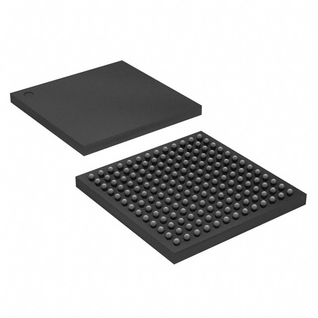
Figure 2: 10M16SAU169I7G in 169-UBGA package – product photo.
4. Typical Applications & Circuit Design
The 10M16SAU169I7G is designed for a wide range of embedded and industrial applications where non-volatile instant-on capability, integrated ADC, and low power consumption are critical. Typical application areas include:
- Industrial Automation – Motor control, sensor interfaces, protocol bridging (Modbus, EtherCAT, PROFINET)
- IoT Edge Computing – Sensor fusion, low-latency data preprocessing, local inference acceleration
- Embedded Vision – Camera interface, video scaling, image pre-processing pipelines
- Automotive Systems – ADAS sensor aggregation, dashboard displays, body control modules
- Medical Devices – Portable diagnostic equipment, patient monitoring, signal conditioning
- Communications – Protocol conversion, SDR front-ends, baseband processing
- Consumer Electronics – Display controllers, audio processing, peripheral bridges
The integrated dual 12-bit ADC is especially valuable for mixed-signal applications, allowing direct sampling of analog sensors without external ADC ICs. Combined with DDR3 memory interface support and up to 549 Kb of embedded memory, the 10M16SAU169I7G provides a highly integrated single-chip solution.

Figure 3: MAX 10 FPGA Development Kit – demonstrating a typical system-level application circuit.
5. Development Tools & Resources
Intel provides a comprehensive ecosystem for developing with the MAX 10 FPGA family:
- Quartus Prime Lite Edition – Free FPGA design software supporting synthesis, place-and-route, timing analysis, and programming for all MAX 10 devices
- Platform Designer (Qsys) – System integration tool for building Nios II soft processor systems with peripherals and memory controllers
- ModelSim-Intel Edition – RTL simulation tool included free with Quartus Prime Lite
- MAX 10 FPGA Development Kit – Full-featured evaluation board with 50K LE MAX 10 device, DDR3, HSMC, Pmod connectors
- MAX 10 Evaluation Kits – Low-cost boards featuring 10M08 devices for quick prototyping
- Nios II Embedded Processor – Soft-core processor IP for building complete embedded systems on the FPGA
The MAX 10 supports both JTAG and internal flash configuration methods, with dual-image support enabling safe remote firmware updates. The device powers up in less than 10 ms from internal flash, and a sleep mode with < 1 ms wake-up time enables aggressive power management strategies.
Video Tutorial: Getting Started with MAX 10 FPGA
6. Frequently Asked Questions (FAQ)
What is the difference between 10M16SAU169I7G and 10M16SAU169C8G?
The main differences are temperature grade and speed grade. The 10M16SAU169I7G is an industrial-grade device rated for -40°C to +100°C with speed grade 7, while the 10M16SAU169C8G is a commercial-grade device rated for 0°C to +85°C with speed grade 8 (slower). The "I" suffix indicates industrial, and "C" indicates commercial temperature range.
Does the 10M16SAU169I7G require an external configuration memory?
No. The MAX 10 FPGA family features internal configuration flash memory, eliminating the need for external configuration devices such as EEPROMs or serial flash. The device stores its configuration internally and loads automatically at power-up in less than 10 ms. It even supports dual configuration images for safe remote updates.
What software is needed to program the 10M16SAU169I7G?
You need Intel Quartus Prime Lite Edition, which is available as a free download from Intel/Altera. It supports all MAX 10 devices and includes synthesis, place-and-route, timing analysis, and the programmer tool. The software supports both Verilog and VHDL design entry, along with schematic capture and IP integration through Platform Designer.
How many ADC channels does the 10M16SAU169I7G have?
The 10M16SAU169I7G contains a dual 12-bit analog-to-digital converter (ADC) capable of up to 1 MSPS sampling rate. The number of available ADC input channels depends on the package variant; in the U169 package, dedicated analog input pins are provided for direct sensor measurement without external ADC components.
Can the 10M16SAU169I7G interface with DDR3 memory?
Yes. The MAX 10 FPGA family supports DDR3, DDR2, LPDDR2, and SRAM external memory interfaces. However, the U169 package has a limited number of I/O pins (130), so the available memory interface width may be constrained compared to larger package variants like U324 or F484. Careful pin planning is recommended when implementing DDR3 in this package.
What are the power supply requirements for the 10M16SAU169I7G?
The 10M16SAU169I7G requires a 1.2V core supply (VCC) for the FPGA fabric, plus I/O bank supplies (VCCIO) that can range from 1.2V to 3.3V depending on the I/O standard used. Additionally, a 2.5V analog supply (VCCA) is needed for the PLLs and ADC. A dedicated 3.3V supply may be required for specific I/O banks. Intel provides detailed power estimation tools in Quartus Prime to help size power supplies accurately.
Related Products on wwdparts.com
- Browse All Semiconductor Components at wwdparts
- Shop FPGA & Programmable Logic Devices
- Read More Technical Articles on the wwdparts Blog


