
Request a Quote · 10M16SAU169I7G

MAX 10 FPGA Development Kit Block Diagram — Architecture overview showing FPGA core, memory interfaces, ADC, and peripheral connectivity (Source: Altera/Intel)
The 10M16SAU169I7G is a non-volatile FPGA from Intel (formerly Altera) belonging to the MAX 10 device family. Built on 55nm flash technology, it integrates 16,000 logic elements, 549 Kb of embedded memory, 45 embedded 18×18 multiplier DSP blocks, and dual analog-to-digital converters—all within a compact 169-ball UBGA package. With an industrial temperature range of −40°C to +100°C and instant-on capability from internal configuration flash, the 10M16SAU169I7G is engineered for cost-sensitive industrial IoT, motor control, sensor fusion, and embedded vision applications where single-chip integration, reliability, and low power consumption are paramount.
Table of Contents
1. Overview and Core Features
The Intel MAX 10 family represents a breakthrough in non-volatile FPGA design, combining a true single-chip programmable logic solution with integrated flash memory for instant-on operation. The 10M16SAU169I7G sits in the mid-range of the MAX 10 lineup, offering 16,000 logic elements organized into 1,000 logic array blocks (LABs) of 16 LEs each. Unlike SRAM-based FPGAs that require external configuration memory, the MAX 10 stores its bitstream in on-chip dual-boot flash, enabling the device to begin operating within milliseconds of power-up.
Key differentiators of the 10M16SAU169I7G include its integrated dual analog-to-digital converters (ADCs) with up to 18 analog input channels and 12-bit resolution at 1 MSPS, enabling direct sensor interfacing without external ADC ICs. The device provides 549 Kb of embedded M9K SRAM blocks, four phase-locked loops (PLLs) for flexible clock management, and 45 embedded 18×18 multiplier blocks for DSP-intensive operations such as digital filtering and motor control algorithms. With 130 user I/O pins in the compact 11×11 mm UBGA-169 package, the device supports LVTTL, LVCMOS, SSTL, HSTL, and LVDS I/O standards, along with DDR3 and DDR2 external memory interfaces.
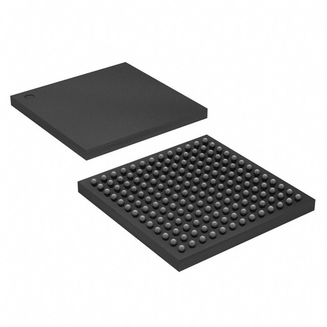
10M16SAU169I7G UBGA-169 Package — 11×11 mm BGA with 130 user I/O pins (Source: Microchip USA)
2. Specifications and Parameter Table
| Parameter | Value |
|---|---|
| Manufacturer | Intel (formerly Altera) |
| Device Family | MAX 10 (Non-Volatile FPGA) |
| Logic Elements (LEs) | 16,000 |
| Logic Array Blocks (LABs) | 1,000 |
| Embedded Memory (M9K) | 549 Kb (562,176 bits) |
| Embedded 18×18 Multipliers | 45 |
| PLLs | 4 |
| User I/O Pins | 130 |
| Maximum LVDS Pairs | 22 |
| Analog-to-Digital Converter | Dual ADC, 12-bit, up to 1 MSPS |
| Internal Configuration | Dual-boot flash (instant-on) |
| User Flash Memory (UFM) | Yes |
| External Memory Interface | DDR3, DDR2, LPDDR2 |
| I/O Standards | 3.3V/2.5V/1.8V/1.5V/1.2V LVCMOS, LVTTL, SSTL, HSTL, LVDS |
| Core Voltage | 1.2 V |
| I/O Supply Voltage | 3.0 V to 3.3 V |
| Process Technology | 55 nm Flash |
| Speed Grade | 7 (Industrial) |
| Package | UBGA-169 (11×11 mm) |
| Operating Temperature | −40°C to +100°C (Industrial) |
| Mounting Type | Surface Mount (SMD/SMT) |
| FPGA Bitstream Security | AES-256 encryption |
| RoHS Compliance | RoHS Compliant |
Looking for 10M16SAU169I7G Inventory?
Check our real-time stock levels, pricing, and volume discounts for global distribution.
Check 10M16SAU169I7G Stock3. Architecture, Pinout, and Application Circuit
The MAX 10 architecture centers on a sea of 16 logic elements (LEs) per LAB, interconnected through a column-and-row routing fabric. Each LE contains a 4-input look-up table (LUT), a programmable register, and carry chain logic for efficient arithmetic operations. The 549 Kb of M9K embedded memory is organized in 9 Kb blocks, each configurable as single-port RAM, dual-port RAM, FIFO, ROM, or shift register. The 45 embedded multiplier blocks can be configured as 18×18-bit or dual 9×9-bit multipliers, delivering up to 90 independent multiply-accumulate operations for DSP workloads.
The 10M16SAU169I7G in the UBGA-169 package provides 130 general-purpose I/O pins organized into multiple I/O banks supporting mixed-voltage operation. The four PLLs support frequency synthesis from 5 MHz to 472.5 MHz with up to five output counters each, enabling complex clocking schemes for multi-domain designs. The dual integrated ADCs share up to 18 analog input channels, each with 12-bit resolution at sampling rates up to 1 MSPS—ideal for temperature monitoring, voltage supervision, and sensor data acquisition without external ADC components.
For the reference design, Intel recommends a regulated 1.2V supply for the FPGA core with 3.3V for I/O banks, using multiple decoupling capacitors (100 nF ceramic and 10 µF tantalum) placed close to each VCC and VCCIO pin. JTAG and Active Serial programming interfaces are supported, with the dual-boot flash enabling in-field firmware updates through remote configuration schemes.

MAX 10 FPGA Development Kit — Reference application platform featuring DDR3 memory, ADC analog inputs, HSMC expansion, and Arduino headers (Source: Altera/Intel)
4. Video: MAX 10 FPGA Design Tutorial
This video covers the essentials of getting started with MAX 10 FPGA development using Intel Quartus Prime. Topics include project setup, pin assignment, design compilation, and programming the MAX 10 device—directly applicable to designs utilizing the 10M16SAU169I7G in UBGA-169 package.
5. Equivalents, Cross-Reference, and Lifecycle
The 10M16SAU169I7G carries an Active production status from Intel/Altera with no announced end-of-life date. The device is available in tray packaging. For designs requiring different specifications, speed grades, or temperature ranges within the same family, engineers should consider:
- 10M16SAU169C8G — Same 16K LE device in UBGA-169 but with commercial temperature range (0°C to +85°C) and speed grade 8. Ideal for cost-sensitive applications not requiring industrial temperature operation.
- 10M08SAE144C8G — A lower-density MAX 10 variant with 8,000 LEs in an EQFP-144 package. Suitable for simpler designs where the full 16K LE capacity is not needed and a leaded package is preferred for prototyping.
- 10M25SAE144C8G — A higher-density MAX 10 option with 25,000 LEs, offering more logic capacity for complex designs while remaining within the same non-volatile FPGA architecture.
- EP4CE10E22C8N — An Altera Cyclone IV FPGA with 10,320 LEs. An alternative when SRAM-based FPGA flexibility is preferred and external configuration memory is acceptable.
When selecting an alternative, verify that the I/O count, memory capacity, PLL resources, and temperature specifications meet your design requirements. The MAX 10 family’s unique advantage lies in its non-volatile instant-on capability and integrated ADC, features not available in Cyclone IV or V devices. Check 10M16SAU169I7G Inventory & Pricing at WWDParts for current lead times and stock availability.
6. Frequently Asked Questions (FAQ)
Q1: What is the 10M16SAU169I7G, and what applications is it designed for?
The 10M16SAU169I7G is a non-volatile FPGA from Intel’s MAX 10 family, featuring 16,000 logic elements in a UBGA-169 package with industrial temperature rating (−40°C to +100°C). It is designed for industrial IoT gateways, motor and power control, sensor hub and data fusion, factory automation, embedded vision preprocessing, LED lighting control, and portable instrumentation where instant-on operation, integrated ADC, and single-chip implementation reduce BOM cost and PCB area.
Q2: How does the MAX 10 instant-on feature work, and why does it matter?
The MAX 10 stores its configuration bitstream in on-chip flash memory rather than external SPI or parallel flash. On power-up, the configuration is loaded from internal flash in under 10 milliseconds, allowing the FPGA to begin operating almost immediately. This is critical for safety-critical and industrial applications where the system must respond within a deterministic startup window. The dual-boot flash also supports storing two separate configuration images, enabling secure in-field firmware updates with automatic fallback to a known-good image if the primary boot fails.
Q3: What are the key differences between the 10M16SAU169I7G (I7G) and 10M16SAU169C8G (C8G) variants?
The “I7G” suffix denotes industrial temperature (−40°C to +100°C) with speed grade 7, while “C8G” indicates commercial temperature (0°C to +85°C) with speed grade 8. Speed grade 7 is the fastest available for industrial devices in this family, offering lower propagation delays and higher clock frequencies than speed grade 8. The I7G variant is preferred for harsh environments such as outdoor equipment, automotive-adjacent systems, and industrial control panels exposed to temperature extremes.
Q4: What design tools and IP cores are available for developing with the 10M16SAU169I7G?
Intel provides the Quartus Prime Lite Edition (free) as the primary development tool, which includes the Platform Designer (formerly Qsys) system integration tool, the Nios II soft processor, and a library of parameterizable IP cores covering DDR3 memory controllers, PCI Express bridges, Ethernet MACs, UART, SPI, I²C, and the ADC IP block. The MAX 10 also supports the Nios II/e economy processor for control-plane tasks, and Intel offers reference designs for the MAX 10 FPGA Evaluation Kit and Development Kit to accelerate prototyping.
Q5: How do I use the integrated ADC in the 10M16SAU169I7G?
The MAX 10 dual ADC block is accessed through the Altera Modular ADC IP core instantiated in Quartus Prime Platform Designer. Each ADC channel provides 12-bit resolution at up to 1 MSPS sampling rate. Analog inputs are routed to dedicated ADC pins on the UBGA-169 package, with input voltage range configurable from 0–2.5V or 0–3.3V depending on the reference voltage configuration. The IP core supports sequencer-based multi-channel scanning, threshold detection, and Avalon-MM register interface for easy integration with Nios II or custom logic. External anti-aliasing filters and voltage dividers may be needed for signals exceeding the input range.
Q6: What power supply design considerations apply to the 10M16SAU169I7G?
The device requires a 1.2V core supply (VCCINT), 2.5V PLL analog supply (VCCA), and 3.0V–3.3V I/O bank supply (VCCIO). Intel recommends using dedicated low-noise LDO regulators or DC-DC converters for each rail, with 100 nF ceramic decoupling capacitors placed at every power pin and bulk 10–47 µF capacitors per power island. Power sequencing should bring VCCINT up first, followed by VCCIO and VCCA. The Intel Power Management reference design and Early Power Estimator spreadsheet help calculate power consumption for specific design utilization levels.


