
The 10M16SAU169I7G is a non-volatile FPGA from Intel (formerly Altera) belonging to the MAX 10 family. Built on 55nm flash process technology, it delivers 16,000 logic elements with an integrated 12-bit ADC, user flash memory, and dual-configuration support — all in a compact UBGA-169 package. This guide covers its complete specifications, pinout, block diagram, typical application circuits, and design resources.
Table of Contents
- Key Specifications & Parameters
- Block Diagram & Architecture
- Pinout & Package Information
- Application Circuits & Design Examples
- Video Tutorial & Development Resources
- Frequently Asked Questions
Key Specifications & Parameters
The following table summarizes the core electrical and functional parameters of the 10M16SAU169I7G. For full parametric data, refer to the official Intel/Altera MAX 10 datasheet.
| Parameter | Value |
|---|---|
| Manufacturer | Intel (Altera) |
| Family | MAX 10 |
| Part Number | 10M16SAU169I7G |
| Logic Elements (LEs) | 16,000 |
| Logic Array Blocks (LABs) | 1,000 |
| Embedded Memory (M9K RAM) | 549 Kbits |
| Total RAM Bits | 562,176 |
| User Flash Memory (UFM) | 736 Kbits |
| 18×18 Embedded Multipliers | 45 |
| PLLs | 4 |
| ADC | 1× 12-bit SAR, up to 1 MSPS, 17 channels |
| User I/O Pins | 130 |
| Max Operating Frequency | 450 MHz |
| Core Supply Voltage | 1.2 V |
| I/O Supply Voltage | 3.0 V / 3.3 V |
| Operating Temperature | −40°C to +100°C (Industrial) |
| Speed Grade | 7 |
| Package | UBGA-169 (11 mm × 11 mm, 0.8 mm pitch) |
| Process Technology | 55 nm Flash |
| Configuration | Internal flash (dual-image boot) |
| RoHS Compliant | Yes (Lead-Free) |
Block Diagram & Architecture
The MAX 10 architecture integrates configurable logic, embedded memory, DSP blocks, PLLs, a 12-bit ADC, and flash memory on a single die. The block diagram below illustrates the internal architecture and interconnect of the MAX 10 development platform:
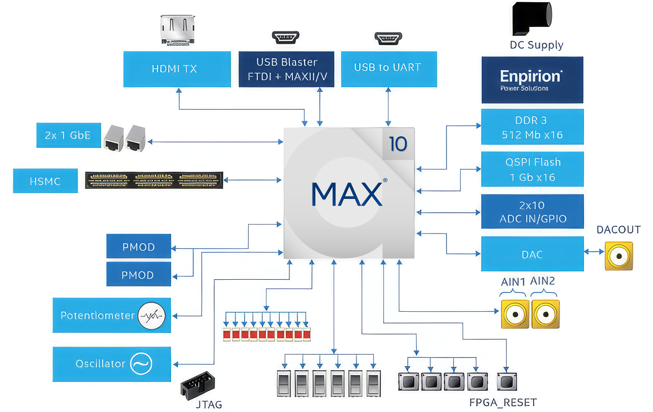
Figure 1: MAX 10 FPGA Development Kit System Block Diagram
Key architectural highlights of the 10M16SAU169I7G include:
- Logic Array Blocks (LABs): 1,000 LABs, each containing 16 adaptive logic modules (ALMs) equivalent logic elements
- M9K Memory Blocks: Embedded SRAM blocks providing 549 Kbits of on-chip dual-port memory
- DSP Blocks: 45 embedded 18×18 multipliers for signal processing acceleration
- Integrated ADC: 12-bit SAR converter with dedicated analog routing and temperature sensor
- Dual Configuration Flash: Supports two configuration images for remote update and fail-safe boot
Pinout & Package Information
The 10M16SAU169I7G is housed in a 169-ball UBGA (Ultra Fine-pitch Ball Grid Array) package. With 130 user I/O pins, it supports multiple I/O standards including LVTTL, LVCMOS, SSTL, HSTL, and LVDS differential signaling. The compact 11 mm × 11 mm footprint makes it well-suited for space-constrained designs.

Figure 2: 10M16SAU169I7G UBGA-169 Package
Pin assignment considerations for the UBGA-169 package:
- Power Pins: Dedicated VCC (1.2V core), VCCIO (3.0V/3.3V), and GND balls
- JTAG Pins: TCK, TDI, TDO, TMS for programming and debug
- Configuration Pins: nSTATUS, nCONFIG, CONF_DONE for boot control
- ADC Input Pins: Dedicated analog input pins for the integrated 12-bit ADC
- Clock Inputs: Dedicated clock input pins routed to the 4 on-chip PLLs
For complete pin tables and I/O bank assignments, download the official pin-out file from the Intel Quartus Pin Planner.
Application Circuits & Design Examples
The MAX 10 FPGA is widely used in industrial control, sensor interfacing, communication bridging, and embedded processing. The image below shows a typical MAX 10 FPGA development and evaluation platform with peripheral interfaces:
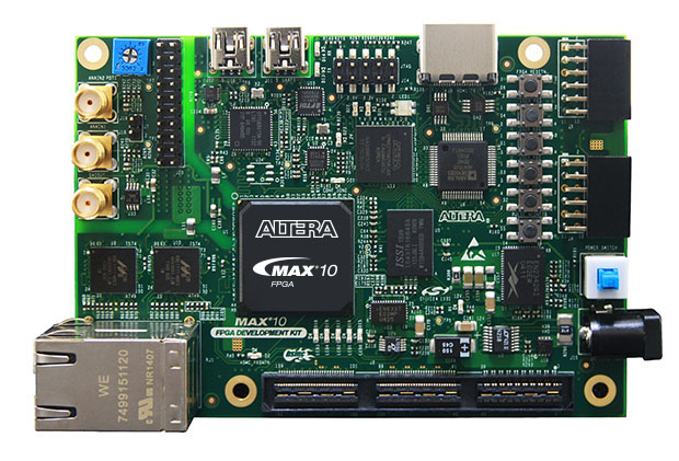
Figure 3: MAX 10 FPGA Development Kit – Top View
Typical application areas for the 10M16SAU169I7G:
- Industrial Automation: Motor control, PLC co-processing, and real-time sensor data acquisition using the built-in 12-bit ADC
- IoT Edge Computing: Protocol bridging (SPI, I2C, UART), data aggregation, and lightweight encryption
- Communications: LVDS serializer/deserializer, Ethernet MAC integration, and custom protocol engines
- Power Management: Digital power supply control, PMBus interface, and voltage/current monitoring via ADC
- Embedded Processing: Nios II soft processor core with up to 549 Kbits on-chip SRAM and external memory interfaces
Video Tutorial & Development Resources
The following video provides an introduction to developing with Intel MAX 10 FPGAs, covering Quartus Prime setup, pin assignment, and basic design flow:
Essential development resources:
- Quartus Prime Lite Edition: Free FPGA design software supporting MAX 10 devices
- Platform Designer (Qsys): System integration tool for Nios II and peripheral IP cores
- ModelSim Intel Edition: RTL simulation and verification
- USB-Blaster II: JTAG programming cable for device configuration and debug
- Browse more FPGA components at WWDParts
Frequently Asked Questions
What is the 10M16SAU169I7G?
The 10M16SAU169I7G is an Intel (Altera) MAX 10 family FPGA featuring 16,000 logic elements, an integrated 12-bit SAR ADC, and user flash memory in a compact 169-ball UBGA package. It is designed for industrial-grade applications with a −40°C to +100°C operating temperature range.
What package type does the 10M16SAU169I7G use?
The 10M16SAU169I7G uses a UBGA-169 (Ultra Fine-pitch Ball Grid Array) package with 169 balls, measuring 11 mm × 11 mm with a 0.8 mm ball pitch and 1.55 mm height.
Does the 10M16SAU169I7G have an integrated ADC?
Yes, the 10M16SAU169I7G includes an integrated 12-bit successive approximation register (SAR) ADC with up to 17 analog input channels and a cumulative sampling rate of up to 1 MSPS. It also features an on-chip temperature sensor.
What is the maximum operating frequency of the 10M16SAU169I7G?
The 10M16SAU169I7G supports a maximum operating frequency of up to 450 MHz, depending on the design and routing. The speed grade is 7, which is the industrial-grade speed specification.
What development tools are needed for the 10M16SAU169I7G?
You need Intel Quartus Prime Lite Edition (free) or Quartus Prime Standard/Pro Edition for FPGA design. Programming is done via JTAG using a USB-Blaster or USB-Blaster II. The MAX 10 also supports internal configuration from its built-in flash memory.
What are common applications for the 10M16SAU169I7G MAX 10 FPGA?
Common applications include industrial automation and control systems, motor drive interfaces, sensor data acquisition (using the built-in ADC), embedded processing, communications protocol bridging, IoT edge computing, and power management systems.


