
The 10M16SAU169I7G is a versatile FPGA from the Intel (formerly Altera) MAX 10 family. Built on 55nm non-volatile flash technology, this device integrates 16,000 logic elements, embedded memory, analog-to-digital converters (ADC), and internal configuration flash into a compact 169-pin UBGA package. Its industrial-grade temperature range (-40°C to +100°C) and low power consumption make it ideal for cost-sensitive industrial, automotive, and IoT applications. This comprehensive guide covers its specifications, pinout, block diagram, application circuits, and frequently asked questions to help engineers evaluate and design with the 10M16SAU169I7G.
Key Specifications & Parameters
The following table summarizes the critical electrical and functional parameters of the 10M16SAU169I7G MAX 10 FPGA. Engineers should reference the official Altera FPGA documentation for comprehensive timing and electrical data.
| Parameter | Value |
|---|---|
| Manufacturer | Intel (Altera) |
| Family | MAX 10 FPGA |
| Part Number | 10M16SAU169I7G |
| Logic Elements (LEs) | 16,000 |
| Logic Array Blocks (LABs) | ~1,000 |
| Embedded Memory (RAM) | 549 Kb (562,176 bits) |
| Phase-Locked Loops (PLLs) | 4 |
| User I/O Pins (U169) | 130 |
| 18×18 Embedded Multipliers | 45 |
| Analog-to-Digital Converter (ADC) | Yes (12-bit, dual ADC) |
| Internal Flash Memory | Yes (User Flash + Configuration Flash) |
| External Memory Interface | DDR2, DDR3, LPDDR2, SRAM |
| Process Technology | 55 nm |
| Core Supply Voltage | 1.2 V |
| I/O Supply Voltage | 3.0 V – 3.3 V |
| I/O Standards Supported | LVTTL, LVCMOS, SSTL, HSTL, HSUL, LVDS, PCI |
| Speed Grade | 7 (Slowest) |
| Operating Temperature | -40°C to +100°C (Industrial) |
| Package | 169-Pin UBGA (Ultra-thin BGA) |
| Mounting | SMD/SMT |
| RoHS Compliant | Yes |
Block Diagram & Architecture
The MAX 10 FPGA architecture integrates logic elements, embedded memory blocks (M9K), DSP blocks with 18×18 multipliers, PLLs, ADC blocks, and user flash memory into a single chip. The internal configuration flash eliminates the need for an external configuration device, enabling instant-on functionality. Below is the block diagram illustrating the system-level integration of the MAX 10 platform:
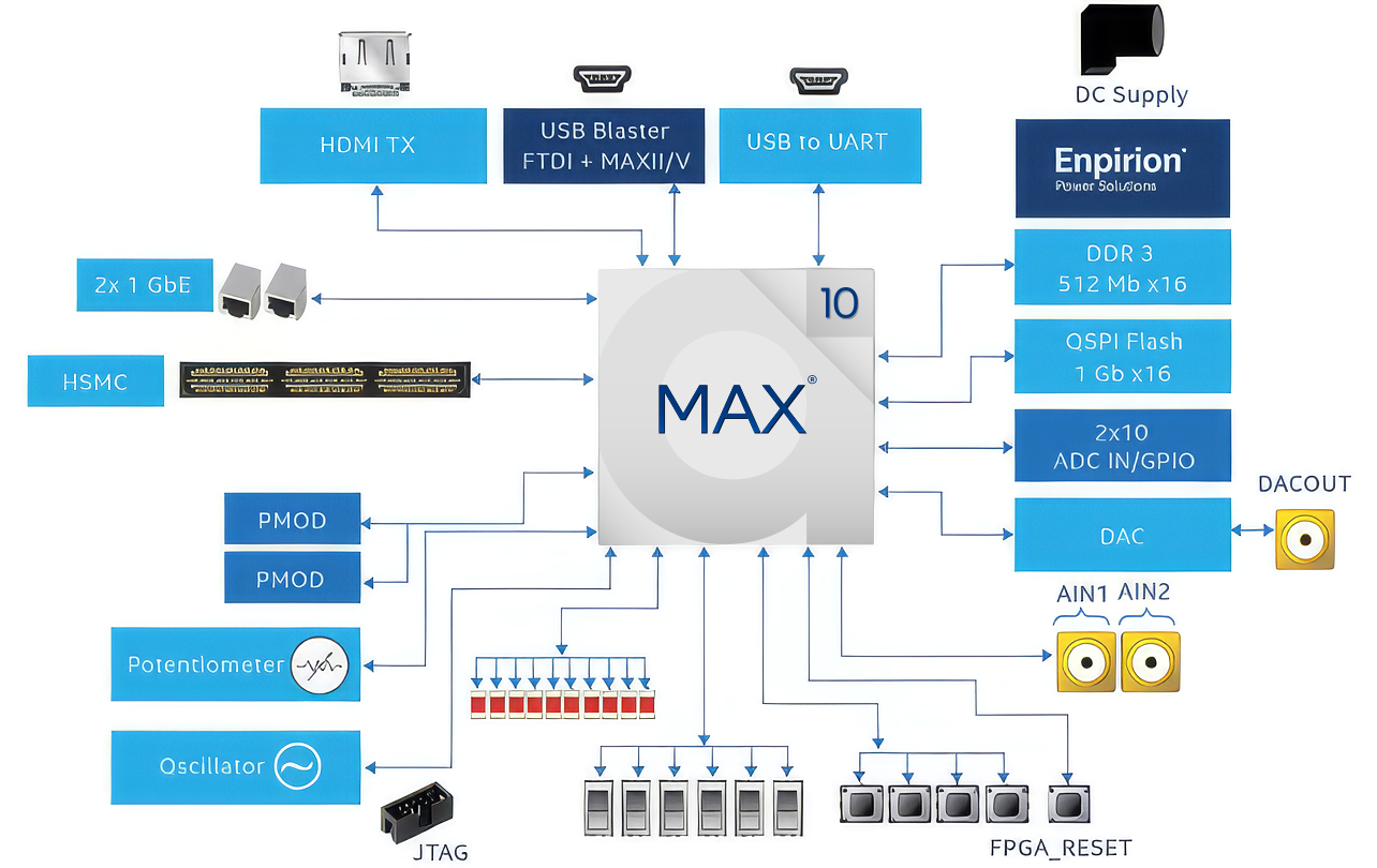
Figure 1: Intel MAX 10 FPGA block diagram and system architecture overview.
Pinout & Package Information
The 10M16SAU169I7G uses a 169-ball Ultra-thin Ball Grid Array (UBGA) package with a compact form factor suitable for space-constrained designs. The U169 package provides 130 user I/O pins supporting multiple voltage standards. For detailed pin assignments and bank mapping, refer to the FPGA I/O Pin Planning Guide.
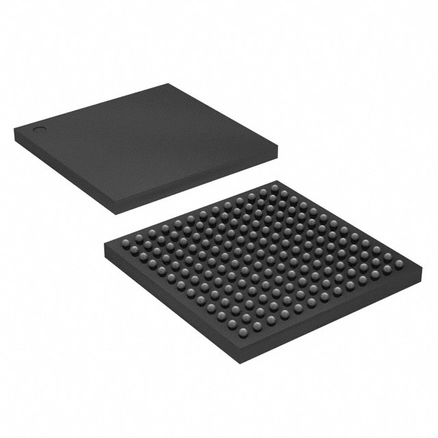
Figure 2: 10M16SAU169I7G physical package – 169-pin UBGA form factor.
Application Circuit & Design Guide
Designing with the 10M16SAU169I7G involves configuring power supplies (1.2V core, 2.5V PLL, 3.3V I/O), connecting the JTAG programming interface, and integrating external memory if needed. The internal flash configuration enables instant-on operation without external EEPROM. The dual ADC blocks allow direct analog sensor interfacing, reducing overall BOM cost. Refer to the FPGA Power Supply Design Tips for best practices on power delivery network design.
Key Design Considerations:
- Power Sequencing: Apply VCCINT (1.2V) before VCCIO (3.3V) to avoid latch-up.
- Decoupling Capacitors: Place 100nF ceramic capacitors close to each VCC pin, plus bulk 10µF capacitors per power rail.
- JTAG Interface: Connect TCK, TDI, TDO, TMS with appropriate pull-up/pull-down resistors.
- Configuration: No external flash needed – internal dual-boot configuration supports remote firmware update.
- ADC Input: Use a low-pass filter on analog input pins for best ADC measurement accuracy.
Video Tutorial
Watch this tutorial to learn how to get started with the Intel MAX 10 FPGA evaluation kit, including Quartus Prime setup, pin assignment, and first project compilation:
Video: Getting started with Intel MAX 10 FPGA development kit and Quartus Prime.
Frequently Asked Questions (FAQ)
What is the 10M16SAU169I7G and what family does it belong to?
The 10M16SAU169I7G is a non-volatile FPGA from the Intel (Altera) MAX 10 family. It features 16,000 logic elements, built-in flash memory for instant-on configuration, and a 12-bit dual ADC – all in a compact 169-pin UBGA package. The "I7G" suffix indicates industrial temperature grade (-40°C to +100°C) with speed grade 7.
Does the 10M16SAU169I7G require an external configuration memory?
No. The MAX 10 FPGA integrates internal configuration flash memory, eliminating the need for an external EEPROM or flash chip. This enables instant-on operation at power-up and supports dual-boot configuration for safe remote firmware updates.
What development tools are needed for the 10M16SAU169I7G?
You can develop with Intel Quartus Prime Lite Edition, which is free and fully supports MAX 10 devices. The toolchain includes the Quartus Prime software for design entry, synthesis, place-and-route, and programming via USB-Blaster JTAG. The Platform Designer (formerly Qsys) tool enables system integration with Nios II soft processors.
What is the operating temperature range and speed grade of the 10M16SAU169I7G?
The 10M16SAU169I7G operates over the industrial temperature range of -40°C to +100°C. It has a speed grade of 7, which is the slowest speed grade in the MAX 10 family. For timing-critical applications, consider the speed grade 6 variant (10M16SAU169C8G) which offers faster performance.
Can the 10M16SAU169I7G interface with DDR3 memory?
Yes. The MAX 10 FPGA family supports DDR2, DDR3, LPDDR2, and SRAM external memory interfaces. However, the U169 package has limited I/O pins (130), so the available memory interface width may be constrained. For wider DDR3 interfaces, consider larger package variants like the F484 or U324.
What are typical applications for the 10M16SAU169I7G?
Common applications include industrial automation and control, motor drive interfaces, sensor data acquisition (leveraging the built-in ADC), IoT edge computing, video and image processing pipelines, communication protocol bridging, and low-cost prototyping. Its non-volatile instant-on capability is particularly valuable in safety-critical industrial systems.


