
The 10M16SAU169I7G is a non-volatile FPGA from the Intel (Altera) MAX 10 family, offering 16,000 logic elements in a compact 169-UBGA package. Built on 55nm flash technology, this industrial-grade device integrates analog-to-digital converters, embedded memory, and user flash memory—eliminating the need for external configuration devices. It is widely used in system management, I/O expansion, motor control, and sensor interface applications.
Table of Contents
- Key Specifications & Parameters
- Block Diagram & Architecture
- Pinout & Package Information
- Application Circuit & Design
- Video Tutorial
- Frequently Asked Questions
Key Specifications & Parameters
The 10M16SAU169I7G delivers a robust feature set for cost-sensitive embedded designs. Below is a comprehensive summary of its core parameters based on official Intel/Altera datasheets.
| Parameter | Value |
|---|---|
| Manufacturer | Intel (Altera) |
| Family | MAX 10 FPGA |
| Logic Elements (LEs) | 16,000 |
| Logic Array Blocks (LABs) | 1,000 |
| Total RAM Bits | 562,176 (549 Kb) |
| Embedded Multipliers (18×18) | Up to 144 |
| PLLs | 4 |
| User I/O Pins | 130 |
| ADC Blocks | Dual 12-bit ADC |
| User Flash Memory (UFM) | Yes (Internal Configuration) |
| Package Type | 169-UBGA (11×11 mm) |
| Supply Voltage | 2.85V – 3.465V (3.3V nominal) |
| Operating Temperature | -40°C to +100°C (TJ) – Industrial |
| Speed Grade | 7 |
| Process Technology | 55nm Flash |
| External Memory Support | DDR2, DDR3, LPDDR2, SRAM |
| I/O Standards | LVTTL, LVCMOS, SSTL, HSTL, LVDS, RSDS, and more |
| RoHS Compliant | Yes |
Block Diagram & Architecture
The MAX 10 architecture integrates logic array blocks (LABs), M9K embedded memory blocks, embedded multipliers, PLLs, a dual analog-to-digital converter, and user flash memory (UFM) into a single non-volatile FPGA. Each LAB contains 16 logic elements (LEs), where each LE features a 4-input look-up table (LUT), a programmable register, and dedicated carry chain logic. The internal flash configuration memory enables instant-on operation without external boot devices.
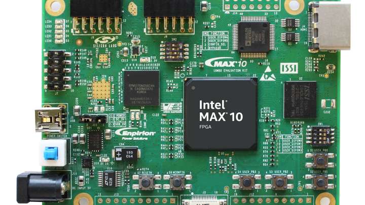
Figure 1: Intel MAX 10 FPGA Architecture Block Diagram
Pinout & Package Information
The 10M16SAU169I7G comes in a 169-ball Ultra Fine-pitch Ball Grid Array (UBGA) package measuring 11×11 mm. This compact footprint makes it suitable for space-constrained designs. The device provides 130 user I/O pins with support for up to 22 LVDS differential pairs, multiple single-ended I/O standards (1.0V to 3.3V LVCMOS/LVTTL), and DDR memory interfaces. All power and ground balls are strategically positioned for optimal signal integrity and thermal performance.
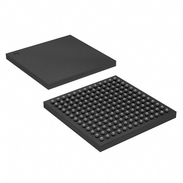
Figure 2: 10M16SAU169I7G 169-UBGA Package Photo
Application Circuit & Design
The 10M16SAU169I7G is ideal for a wide range of embedded applications including industrial automation, motor control, sensor fusion, communication protocol bridging, and I/O expansion. Intel offers the MAX 10 FPGA Development Kit featuring dual Gigabit Ethernet, HDMI output, USB-to-UART, HSMC connector, and dual ADC SMA inputs. The evaluation board includes an op-amp based analog input filtering circuit that scales Arduino-compatible 5.0V signals down to the MAX 10 ADC's 2.5V maximum input voltage. Typical design flow uses Quartus Prime software with VHDL or Verilog HDL.

Figure 3: MAX 10 FPGA Development Kit – Application Reference Board
Video Tutorial
Watch this tutorial to learn more about getting started with Intel MAX 10 FPGA development, including Quartus Prime setup and hardware configuration:
Frequently Asked Questions
What is the 10M16SAU169I7G?
The 10M16SAU169I7G is a non-volatile FPGA from Intel's (Altera) MAX 10 family. It features 16,000 logic elements, dual 12-bit ADCs, 549 Kb of embedded memory, and 130 user I/O pins in a compact 169-UBGA package. It operates across the industrial temperature range of -40°C to +100°C.
What package type does the 10M16SAU169I7G use?
This device uses a 169-ball Ultra Fine-pitch Ball Grid Array (UBGA) package measuring 11×11 mm. The compact BGA form factor is ideal for space-constrained PCB layouts while providing excellent electrical and thermal performance.
Does the 10M16SAU169I7G require an external configuration memory?
No. The MAX 10 family features internal flash-based configuration memory, enabling instant-on operation. The device stores its configuration in on-chip non-volatile memory, eliminating the need for external EEPROM or flash devices and reducing both BOM cost and board space.
What are the main applications for the 10M16SAU169I7G?
Common applications include system management, I/O expansion, motor control, sensor interface and fusion, communication protocol bridging, industrial automation, automotive systems, and consumer electronics. The built-in ADC makes it particularly suitable for mixed-signal designs requiring analog input processing.
What development tools are needed for the 10M16SAU169I7G?
Intel's Quartus Prime Lite Edition (free) supports the MAX 10 family. It includes synthesis, place-and-route, timing analysis, and the built-in ModelSim simulator. Programming is done via USB-Blaster or USB-Blaster II JTAG interfaces. The Nios II soft processor can also be instantiated for embedded software development.
What is the difference between 10M16SAU169I7G and 10M16SAU169C8G?
Both share the same 16,000 LE MAX 10 die in a 169-UBGA package. The key differences are: the "I7G" variant operates across the industrial temperature range (-40°C to +100°C) with speed grade 7, while the "C8G" variant is rated for commercial temperature range (0°C to +85°C) with speed grade 8. Choose the I7G for harsh environment or automotive applications.
Looking for more semiconductor components? Browse our selection of Altera FPGAs, Intel programmable devices, and FPGA development solutions at wwdparts.com.


