
10M16SAU169I7G Intel (Altera) MAX 10 FPGA: Datasheet, Pinout, Specifications & Application Guide
1. Overview of the 10M16SAU169I7G MAX 10 FPGA
The 10M16SAU169I7G is a member of Intel's (formerly Altera) MAX 10 FPGA family, a low-cost, single-chip, non-volatile FPGA built on 55 nm flash technology. Designed for instant-on operation with no external configuration device needed, the MAX 10 series bridges the gap between CPLDs and traditional FPGAs, offering rich programmable logic resources alongside integrated analog-to-digital converters (ADC) and user flash memory.
The 10M16SAU169I7G variant provides 16,000 logic elements (LEs) in a compact UBGA-169 package, rated for the industrial temperature range of -40°C to +100°C. It is an ideal choice for industrial automation, motor control, IoT edge computing, communications infrastructure, and portable instrumentation where reliability, small form factor, and instant-on capability are critical.
As part of the MAX 10 family, this device supports dual configuration images for remote update, integrated ADC blocks for mixed-signal applications, and DDR3 external memory interfaces — all in a single chip solution that simplifies board design and reduces BOM cost.
2. Key Specifications and Parameters
| Parameter | Value |
|---|---|
| Part Number | 10M16SAU169I7G |
| Manufacturer | Intel (Altera) |
| Family | MAX 10 FPGA |
| Logic Elements (LEs) | 16,000 |
| Logic Array Blocks (LABs) | 1,000 |
| Embedded Memory (M9K Blocks) | 549 Kbit (562,176 RAM bits) |
| Embedded 18×18 Multipliers | 45 |
| PLLs | 4 |
| User I/O Pins | 130 |
| ADC Blocks | 1 (Dual ADC, up to 12-bit, 1 MSPS) |
| User Flash Memory | Up to 736 KB (Internal CFM + UFM) |
| External Memory Interface | DDR2, DDR3, LPDDR2, SRAM |
| Maximum LVDS Pairs | 22 |
| I/O Standards | 3.3V / 2.5V / 1.8V / 1.5V LVCMOS, LVTTL, SSTL, HSTL, HSUL, LVDS |
| Core Voltage | 1.2V |
| I/O Voltage | 1.0V – 3.3V |
| Package | UBGA-169 (11 mm × 11 mm) |
| Speed Grade | 7 (Industrial) |
| Operating Temperature | -40°C to +100°C (TJ) |
| Process Technology | 55 nm Flash |
| Configuration | Internal (dual boot, remote update) |
| RoHS Compliant | Yes |
3. Pinout and Package Information
The 10M16SAU169I7G uses the UBGA-169 (U169) package — a 169-ball ultra fine-pitch ball grid array measuring 11 mm × 11 mm with a 0.8 mm ball pitch. This compact BGA package is ideal for space-constrained designs while still providing 130 user I/O pins across multiple I/O banks.
The device organizes its I/O pins into multiple banks, each independently configurable for different voltage standards. This multi-bank architecture enables direct interfacing with 3.3V legacy devices and 1.8V/1.5V modern memory components on the same FPGA. Dedicated pins for JTAG programming (TCK, TDI, TDO, TMS), configuration, and power supply are allocated within the 169-ball footprint.
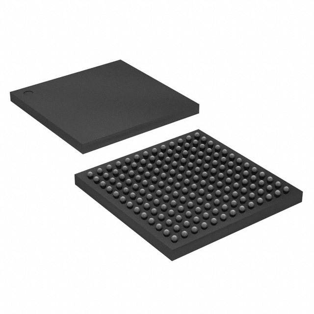
Figure 1: 10M16SAU169I7G in UBGA-169 package — 11 mm × 11 mm BGA with 130 user I/O pins
4. Architecture and Block Diagram
The Intel MAX 10 FPGA architecture integrates several key functional blocks into a single monolithic die:
- Logic Array Blocks (LABs): 1,000 LABs, each containing 16 adaptive logic elements with 4-input LUTs, registers, and carry chain logic.
- Embedded Memory: M9K memory blocks totaling 549 Kbit, configurable as single-port RAM, dual-port RAM, ROM, or FIFO buffers.
- DSP Blocks: 45 embedded 18×18 multipliers for efficient digital signal processing, supporting multiply-accumulate operations for filter implementations.
- Clock Management: 4 PLLs with up to 4 outputs each, supporting frequency synthesis, clock multiplication/division, and phase shifting.
- Analog-to-Digital Converter: Integrated dual ADC block with up to 17 analog input channels, 12-bit resolution at 1 MSPS — enabling true mixed-signal designs without external ADC chips.
- User Flash Memory: Non-volatile on-chip flash for storing configuration data, application code for Nios II soft processors, or user data.
- Instant-On Configuration: Internal flash configuration eliminates the need for external configuration devices, enabling power-on in milliseconds.
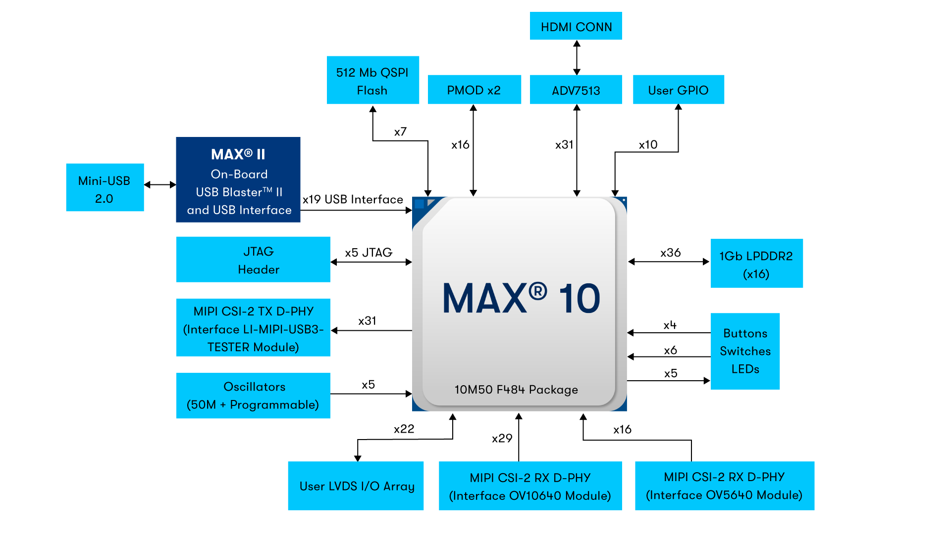
Figure 2: MAX 10 FPGA evaluation kit block diagram — illustrating the integrated architecture with logic, memory, ADC, and I/O resources
5. Typical Applications and Design Considerations
The 10M16SAU169I7G is widely deployed in applications that demand a compact, cost-effective, and reliable FPGA solution with integrated analog capabilities:
- Industrial Automation & Motor Control: Real-time I/O expansion, encoder interfaces, PWM generation, and sensor data acquisition using the integrated ADC.
- IoT Edge Computing: Protocol bridging, sensor fusion, and local data preprocessing at the edge node, leveraging the instant-on capability for always-ready operation.
- Communications Infrastructure: CPRI/OBSAI interface management, clock recovery, and packet processing in small-cell base stations.
- Portable Test & Measurement: High-speed data capture, waveform generation, and signal analysis in handheld instruments where power and space are at a premium.
- Automotive Electronics: ADAS sensor preprocessing, display interface bridging, and body control module logic with industrial-grade temperature support.
When designing with the 10M16SAU169I7G, ensure proper power sequencing (1.2V core before I/O banks), adequate decoupling capacitors on all VCCINT and VCCIO pins, and a robust JTAG interface for in-system programming. The Quartus Prime Lite Edition software (free) fully supports this device for design entry, synthesis, place-and-route, and timing analysis.
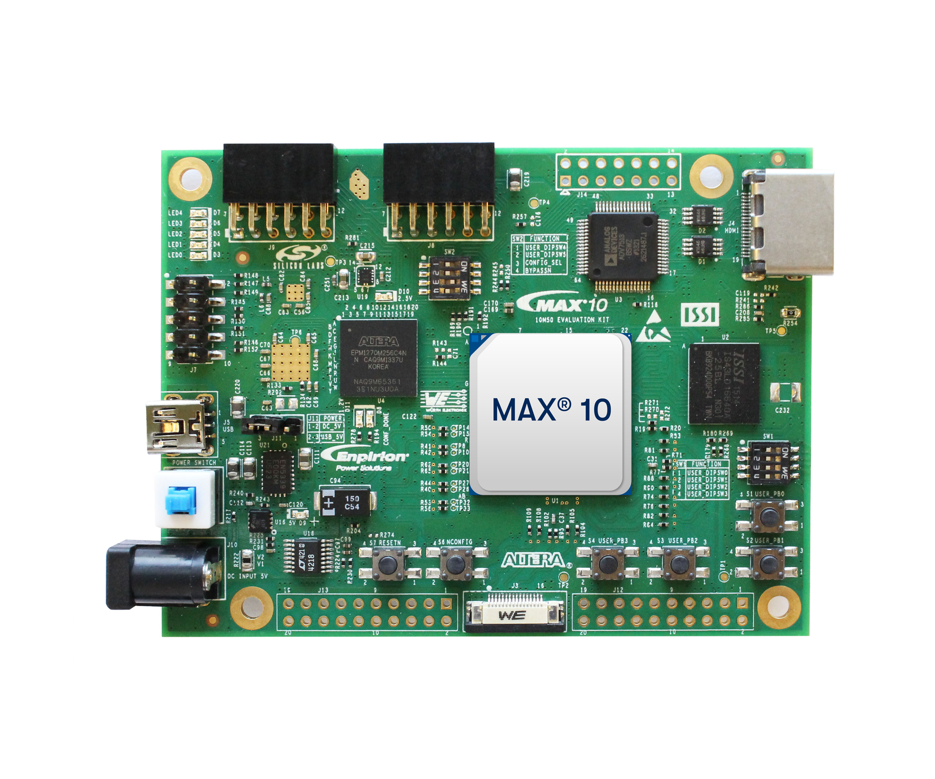
Figure 3: MAX 10 FPGA 10M50 Evaluation Kit — a reference platform for prototyping 10M16SAU169I7G-based designs
Video Tutorial: Getting Started with Intel MAX 10 FPGA
6. Frequently Asked Questions (FAQ)
What is the difference between the 10M16SAU169I7G and 10M16SAU169C8G?
The main differences are temperature range and speed grade. The I7G variant is rated for the industrial temperature range (-40°C to +100°C) with speed grade 7, while the C8G is rated for the commercial temperature range (0°C to +85°C) with speed grade 8 (slower). Choose the I7G for harsh environments, outdoor deployments, or industrial applications requiring extended temperature operation.
Does the 10M16SAU169I7G require an external configuration device?
No. The MAX 10 FPGA family features internal flash-based configuration storage, eliminating the need for an external configuration PROM or flash chip. The device stores up to two configuration images internally, supporting dual-boot and remote update capabilities. This results in instant-on operation (configuration in milliseconds at power-up) and reduced BOM cost.
What software tools are needed to program the 10M16SAU169I7G?
Intel's Quartus Prime Lite Edition (free download) fully supports the MAX 10 device family. It includes schematic entry, Verilog/VHDL design entry, synthesis, place-and-route, timing analysis, and the Programmer tool for JTAG-based device configuration. For embedded soft-processor designs, the Nios II Software Build Tools (included with Quartus Prime) are also available.
Can the 10M16SAU169I7G interface with DDR3 memory?
Yes. The MAX 10 family supports DDR3, DDR2, and LPDDR2 external memory interfaces. The 10M16 device can interface with DDR3 SDRAM at up to 300 MHz (600 Mbps data rate), enabling embedded systems with significant external memory bandwidth. Intel provides the External Memory Interface (EMIF) IP core in Quartus Prime for easy integration.
How many ADC channels does the 10M16SAU169I7G support?
The 10M16SAU169I7G integrates a dual ADC block with up to 17 analog input channels. Each ADC provides 12-bit resolution at up to 1 MSPS (mega samples per second). An internal temperature sensing diode is also available. This integrated ADC eliminates the need for external ADC chips in many mixed-signal applications such as power monitoring, sensor data acquisition, and system health management.
What is the UBGA-169 package and what are its advantages?
The UBGA-169 (Ultra Fine-Pitch Ball Grid Array, 169 balls) is an 11 mm × 11 mm surface-mount package with a 0.8 mm ball pitch. Its advantages include: (1) very small footprint for space-constrained PCB designs, (2) excellent thermal performance due to the BGA's large solder-ball contact area with the board, (3) shorter signal paths for better high-speed signal integrity, and (4) compatibility with standard SMT assembly processes (requires X-ray inspection for quality control).


