
10M16SAU169I7G Datasheet, Pinout, Equivalents, and Specs
The 10M16SAU169I7G is a non-volatile FPGA from Altera's (now Intel) MAX 10 family, fabricated on a 55nm flash process. With 16,000 logic elements, 549 Kb of embedded memory, 45 embedded multipliers, an integrated analog-to-digital converter (ADC), and internal configuration flash, it delivers instant-on capability without an external configuration device. The device ships in a 169-ball UBGA package (11 × 11 mm) at industrial temperature grade (−40 °C to +100 °C) with an I7G speed grade.
What Is the 10M16SAU169I7G?
The 10M16SAU169I7G belongs to the MAX 10 family — Altera's single-chip, non-volatile FPGA line built on TSMC's 55nm embedded flash process. The "M" in the ordering code indicates an FPGA with integrated configuration flash memory, eliminating the need for external serial configuration devices such as EPCS or EPCQ. This instant-on architecture enables the device to begin operating within milliseconds of power-up, making it ideal for applications where boot latency is critical.
Internally the device organizes 16,000 logic elements into 1,000 Logic Array Blocks (LABs), each containing 16 four-input look-up tables (LUTs) and 16 programmable registers. Embedded memory is provided by M9K blocks (each offering 9,216 bits of true dual-port SRAM), totaling 549 Kb of on-chip memory configurable as single-port RAM, dual-port RAM, FIFO buffers, shift registers, or ROM. The 45 embedded multipliers support 18 × 18 multiply operations for DSP-intensive applications such as digital filtering and motor control. Four PLLs provide clock synthesis, multiplication, division, and phase shifting across independent clock domains.
A distinguishing feature of the MAX 10 family is the integrated 12-bit SAR ADC with up to 18 analog input channels, supporting sample rates up to 1 MSPS. This on-chip ADC eliminates the need for external analog front-end components in sensor-interface and power-monitoring designs. The device also includes up to 736 Kb of user flash memory (UFM) for storing application data, calibration parameters, or firmware images.

Pinout Configuration and Packaging
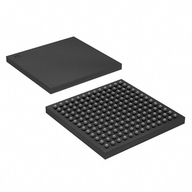
The 10M16SAU169I7G is housed in a 169-ball Ultra FineLine BGA (UBGA) package designated U169 (11 × 11 mm body, 0.8 mm ball pitch). Of the 169 balls, up to 130 are available as general-purpose I/O pins distributed across 8 I/O banks. Each I/O bank supports independent VCCIO supply rails, enabling mixed-voltage interfacing (1.2 V, 1.5 V, 1.8 V, 2.5 V, and 3.3 V) within a single device.
Critical power pins include VCC (1.2 V core supply), VCCIO (per-bank selectable at 1.2 V to 3.3 V), and VCCA (analog PLL and ADC supply at 2.5 V). The configuration flash is internal, so no dedicated configuration pins are needed for normal operation. JTAG pins (TCK, TMS, TDI, TDO) are available for boundary-scan testing and in-system programming via Quartus Prime. The device supports up to 22 LVDS differential pairs for high-speed parallel data transfer, along with DDR2, DDR3, and LPDDR2 external memory interfaces with soft memory controller IP.
Specifications Parameter Table
| Specification | Technical Details |
|---|---|
| Device Family | MAX 10 (Altera / Intel) |
| Logic Elements (LEs) | 16,000 |
| Logic Array Blocks (LABs) | 1,000 |
| Embedded Memory | 549 Kb (M9K blocks) |
| User Flash Memory (UFM) | 736 Kb |
| Embedded Multipliers (18x18) | 45 |
| PLLs | 4 |
| Analog-to-Digital Converter | 12-bit SAR ADC, up to 1 MSPS, 18 channels |
| User I/O Pins | 130 |
| LVDS Pairs | 22 |
| External Memory Interface | DDR2, DDR3, LPDDR2 (soft controller) |
| Package | 169-UBGA, 11 x 11 mm, 0.8 mm pitch |
| Process Node | 55 nm (TSMC embedded flash) |
| Core Voltage (VCC) | 1.2 V |
| I/O Voltage (VCCIO) | 1.2 V to 3.3 V (per bank) |
| Speed Grade | I7G (Industrial) |
| Operating Temperature | -40 C to +100 C (Industrial) |
| I/O Standards | 3.0 V / 3.3 V LVTTL, 1.0 V - 3.3 V LVCMOS, SSTL, HSTL, HSUL, LVDS, PCI |
| Configuration | Internal flash (instant-on), JTAG |
| Mounting | SMD / SMT |
| RoHS Compliant | Yes |
Typical Applications and Circuit Considerations
The 10M16SAU169I7G is widely deployed in designs that require single-chip integration of programmable logic, analog sensing, and non-volatile storage at an optimized power budget and compact footprint. The 55nm flash process enables instant-on operation, while the industrial temperature rating makes the device suitable for harsh-environment deployments. Typical system-level applications include:
- Industrial Automation and Sensor Fusion: The integrated 12-bit ADC directly digitizes analog sensor signals (temperature, pressure, current) without external converters, while the FPGA fabric implements real-time control loops, PID controllers, and communication protocol engines (Modbus, EtherCAT, PROFINET).
- Motor Drive and Power Management: The 45 embedded multipliers accelerate field-oriented control (FOC) and space-vector PWM calculations, while the ADC monitors bus voltage and phase currents. Instant-on capability ensures the drive controller initializes before the power stage.
- Board Management and System Monitor: In server and telecom platforms, the MAX 10 acts as a board management controller (BMC), monitoring supply rails via the ADC, managing power sequencing, and providing a JTAG-accessible register file for out-of-band system diagnostics.
- IoT Edge Gateways and Smart Metering: The compact UBGA-169 package, low standby power, and integrated flash memory support battery-powered and space-constrained IoT endpoints. UFM stores calibration data, encryption keys, or firmware-over-the-air (FOTA) update images.

On the circuit design front, the power distribution network (PDN) requires careful attention: VCC (1.2 V core) should be decoupled with multiple low-ESR ceramic capacitors placed close to the BGA pads, while VCCA (2.5 V analog supply for PLLs and ADC) demands a low-noise LDO regulator with output ripple below 10 mV peak-to-peak. A 3.3 V or 2.5 V VCCIO supply serves the general-purpose I/O banks. The internal configuration flash simplifies BOM and layout by eliminating the external EPCS/EPCQ device, its SPI bus, and associated pull-up resistors.
Equivalents, Cross-Reference, and Lifecycle
Within the MAX 10 family the 10M16SAU169I7G has several pin-compatible and functionally similar variants that designers should consider during part selection or second-source qualification:
| Part Number | Difference |
|---|---|
| 10M16SAU169C8G | Same device, commercial temperature (0 C to 85 C), C8 speed grade |
| 10M16SAE144I7G | Same logic density, 144-EQFP package (20 x 20 mm), industrial temp |
| 10M16SAU324I7G | Same logic density, 324-UBGA package (15 x 15 mm), more I/O (197 pins) |
| 10M08SAU169I7G | Lower density (8,000 LEs), pin-compatible 169-UBGA, industrial temp |
| 10M25SAU324I7G | Higher density (25,000 LEs), 324-UBGA, upward migration path |
The MAX 10 family is in active production status as of 2026. For alternative families, the Lattice ECP5 offers a similar logic-density sweet spot in a non-volatile package, while the Intel Cyclone V provides an upgrade path for designs that outgrow MAX 10 capacity. For sourcing the 10M16SAU169I7G with competitive pricing and guaranteed authenticity, visit the wwdparts.com product page.
Frequently Asked Questions (FAQ)
Does the 10M16SAU169I7G require an external configuration device?
No. The MAX 10 family integrates on-chip configuration flash memory, enabling instant-on operation without an external EPCS or EPCQ serial configuration device. The FPGA loads its bitstream from internal flash within milliseconds of power-up.
What is the resolution and speed of the built-in ADC?
The integrated ADC is a 12-bit successive-approximation register (SAR) converter with a maximum sample rate of 1 MSPS. It supports up to 18 single-ended analog input channels multiplexed into a dual ADC block, with an input voltage range of 0 V to the selected reference voltage.
Is the 10M16SAU169I7G pin-compatible with the 10M16SAU169C8G?
Yes. Both devices share the identical 169-UBGA pinout (11 x 11 mm, 0.8 mm pitch). The I7G variant is rated for industrial temperature (-40 C to +100 C), while the C8G is rated for commercial temperature (0 C to 85 C) and has a slightly different speed grade. The same PCB layout supports both variants.
What development tools are needed to program this FPGA?
The primary tool is Intel Quartus Prime Lite Edition, which is free and supports the MAX 10 family. Design entry can be done in Verilog, VHDL, or schematic capture. Programming is performed via JTAG using an Intel USB-Blaster or USB-Blaster II download cable. The Quartus Platform Designer (formerly Qsys) provides system integration with soft IP cores including Nios II processor, UART, SPI, I2C, and memory controllers.
How much user flash memory (UFM) is available for application data?
The 10M16 device provides up to 736 Kb of user flash memory (UFM) that can be read and written at runtime via the UFM controller IP core. This non-volatile storage is suitable for calibration parameters, encryption keys, boot-loader images, or small data logs that must survive power cycles.
Can the 10M16SAU169I7G interface with DDR3 memory?
Yes. The MAX 10 family supports DDR2, DDR3, and LPDDR2 external memory interfaces through a soft memory controller IP. In the U169 package, the available I/O count (130 pins) may limit the DDR3 data width to x8 or x16. The Quartus Prime IP Catalog provides a configurable memory controller that handles initialization, calibration, and read/write leveling.


