
Request a Quote · 10M16SAU169I7G
Intel MAX 10 FPGA Architecture Block Diagram — Showing LEs, Embedded Memory, ADC Blocks, PLLs, and User I/O (Source: Intel/Altera Datasheet)
The 10M16SAU169I7G is a non-volatile FPGA from Intel (formerly Altera) belonging to the MAX 10 family, built on a 55 nm flash process technology. Featuring 16,000 logic elements, 549 Kb of embedded memory, an integrated dual analog-to-digital converter (ADC), and 4 PLLs, this device delivers instant-on functionality without requiring external configuration memory. Housed in a compact 169-ball UBGA package and rated for the industrial temperature range of −40°C to +100°C with speed grade 7, the 10M16SAU169I7G is engineered for cost-sensitive industrial IoT, motor control, sensor aggregation, and embedded vision applications that demand reliability and rapid power-up.
Table of Contents
1. Overview and Core Features
The Intel MAX 10 family represents the industry’s first single-chip, non-volatile FPGA with integrated flash memory for instant-on operation. The 10M16SAU169I7G variant provides 16,000 logic elements organized in 1,000 logic array blocks (LABs), making it well-suited for mid-density programmable logic applications. Unlike SRAM-based FPGAs that require external flash for configuration, the MAX 10 stores its configuration internally, enabling power-up to user mode in as little as 10 milliseconds.
Key features of the 10M16SAU169I7G include a dual-channel 12-bit SAR ADC capable of 1 MSPS conversion rates, 549 Kb of embedded M9K memory blocks, 16 embedded 18×18-bit multiplier blocks for DSP-intensive applications, and 4 general-purpose PLLs with up to 8 clock outputs. The device supports DDR2, DDR3, and LPDDR2 external memory interfaces, enabling high-bandwidth data storage. With 130 user I/O pins in the UBGA-169 package and support for 3.0 V to 3.3 V LVTTL, LVCMOS, SSTL, HSTL, and LVDS I/O standards, designers have extensive flexibility in interfacing with external peripherals and sensors.

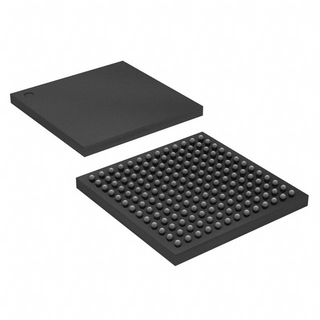
10M16SAU169I7G Package Photo — 169-Ball UBGA (11 mm × 11 mm) Industrial Grade (Source: Digi-Key)
2. Specifications and Parameter Table
| Parameter | Value |
|---|---|
| Manufacturer | Intel (formerly Altera) |
| Family | MAX 10 (10M16) |
| Device Type | Non-Volatile FPGA |
| Logic Elements (LEs) | 16,000 |
| Logic Array Blocks (LABs) | 1,000 |
| Embedded Memory | 549 Kb (M9K blocks) |
| Total RAM Bits | 562,176 |
| Embedded Multipliers (18×18) | 16 |
| PLLs | 4 |
| ADC | Dual 12-bit SAR, up to 1 MSPS |
| User I/O Pins | 130 |
| Maximum LVDS Pairs | 22 |
| External Memory Support | DDR2, DDR3, LPDDR2, SRAM |
| I/O Standards | 3.0–3.3 V LVTTL, 1.0–3.3 V LVCMOS, PCI, SSTL, HSTL, LVDS |
| Configuration | Internal Flash (instant-on, no external config device) |
| Process Technology | 55 nm Flash |
| Supply Voltage | 1.2 V core / 3.0–3.3 V I/O |
| Speed Grade | 7 |
| Operating Temperature | −40°C to +100°C (Industrial) |
| Package | UBGA-169 (11 mm × 11 mm) |
| Mounting | SMD/SMT (Surface Mount) |
| RoHS Compliance | RoHS Compliant |
Looking for 10M16SAU169I7G Inventory?
Check our real-time stock levels, pricing, and volume discounts for global distribution.
Check 10M16SAU169I7G Stock3. Architecture, Pinout, and Application Circuit
The MAX 10 architecture features a regular fabric of logic array blocks (LABs), each containing 16 adaptive logic modules (ALMs) that can implement combinational and sequential functions. The embedded M9K memory blocks provide 9,216-bit dual-port SRAM, configurable as ROM, single-port RAM, dual-port RAM, shift registers, or FIFO buffers. The 16 embedded 18×18-bit multiplier blocks enable efficient implementation of FIR filters, FFTs, and other DSP algorithms without consuming logic resources.
The integrated dual ADC is a standout feature of the MAX 10 family, enabling direct analog sensor interfacing without external ADC chips. Each ADC channel supports up to 17 analog input pins with a 12-bit resolution and 1 MSPS throughput, making it ideal for temperature monitoring, voltage supervision, and sensor data acquisition. The 4 PLLs support clock multiplication, division, and phase shifting with jitter cleaning capability, essential for high-speed serial interfaces and precise timing applications.
The UBGA-169 package provides 130 user I/O pins arranged across multiple I/O banks supporting a variety of single-ended and differential signaling standards. For typical application circuits, the 10M16SAU169I7G requires a 1.2 V core supply, 2.5 V PLL supply, and 3.3 V I/O supply. Decoupling capacitors (0.1 µF and 10 µF) should be placed close to each power pin. The JTAG interface (TCK, TDI, TDO, TMS) enables in-system programming via Intel’s USB-Blaster or compatible programmers.
10M16SAU169I7G Application — Typical Design Implementation with Power Supply and Programming Interface (Source: MicrochipUSA)
4. Video: MAX 10 FPGA Development Tutorial
This video provides a comprehensive walkthrough of Intel MAX 10 FPGA development, covering Quartus Prime project setup, pin assignment, synthesis, and programming via JTAG. The techniques demonstrated apply directly to designs using the 10M16SAU169I7G, including internal flash configuration, ADC integration, and I/O standard selection for the UBGA-169 package.
5. Equivalents, Cross-Reference, and Lifecycle
The 10M16SAU169I7G carries an Active production status from Intel/Altera. The MAX 10 family is supported in the free Quartus Prime Lite Edition, lowering the barrier to entry for evaluation and production. For designs requiring different specifications or alternative packages, consider:
- 10M16SAU169C8G — Same device in commercial temperature range (0°C to +85°C) with speed grade 8. Suitable for consumer and office-environment applications where industrial-grade temperature tolerance is unnecessary.
- 10M16SAE144C8G — The 10M16 in a 144-pin EQFP package with 101 user I/O, offering easier hand-soldering and prototyping compared to the UBGA-169.
- 10M08SAE144C8G — A lower-density MAX 10 variant with 8,000 LEs for applications that need fewer logic resources, reducing cost while retaining the integrated ADC and instant-on capability.
- 10M25SAE144C8G — A higher-density option with 25,000 LEs for more complex designs requiring additional logic and memory resources.
- EP4CE10E22C8N — An Altera Cyclone IV FPGA with similar logic density but SRAM-based configuration, for legacy designs migrating from the Cyclone IV platform.
When selecting an alternative, verify package footprint compatibility, I/O count, and whether the integrated ADC is required. Check 10M16SAU169I7G Inventory & Pricing at WWDParts for current lead times and stock availability.
6. Frequently Asked Questions (FAQ)
Q1: What is the 10M16SAU169I7G, and what is it used for?
The 10M16SAU169I7G is a non-volatile FPGA from Intel’s MAX 10 family, featuring 16,000 logic elements, integrated dual ADC, and internal flash configuration in a 169-ball UBGA package. It is rated for the industrial temperature range (−40°C to +100°C) and is used in industrial IoT gateways, motor control drives, sensor hub aggregation, power management, factory automation, and embedded vision preprocessing applications that require instant power-on operation.
Q2: What does “non-volatile FPGA” mean, and why is instant-on important?
Unlike traditional SRAM-based FPGAs that lose their configuration when power is removed and must reload from external flash at every power-up, the MAX 10 stores its configuration in on-chip flash memory. This means the FPGA is operational within approximately 10 ms of power being applied, without needing an external configuration PROM. Instant-on is critical for safety systems, motor controllers, and industrial equipment where the FPGA must be functional immediately at power-up before an external processor or configuration chain is ready.
Q3: How do I use the integrated ADC on the 10M16SAU169I7G?
The MAX 10 dual ADC provides two independent 12-bit SAR converters with up to 1 MSPS throughput each. You can instantiate the ADC using the Altera IP Catalog in Quartus Prime, selecting the “Modular ADC Core” IP. The ADC supports up to 17 analog input channels (shared across both converters) with a 0 V to reference voltage input range. A dedicated analog supply pin (VREFP) sets the reference voltage. The ADC is ideal for on-board voltage monitoring, temperature sensing, and reading external analog sensors without additional external components.
Q4: What programming tools and configuration methods are supported?
The 10M16SAU169I7G is programmed using Intel Quartus Prime Lite Edition (free) via the JTAG interface with a USB-Blaster or USB-Blaster II programmer. The device supports two configuration modes: JTAG-based configuration for development, and internal configuration from on-chip flash for production deployment. Dual boot images can be stored in the internal flash, enabling a factory fallback image alongside a field-upgradable application image. The device also supports remote system upgrade for in-field firmware updates over a user-defined communication channel.
Q5: What power supplies are required for the 10M16SAU169I7G?
The device requires a 1.2 V core supply (VCC), a 2.5 V PLL analog supply (VCCA), and bank-specific I/O supplies (VCCIO) typically at 3.3 V for LVTTL/LVCMOS interfaces. An analog reference voltage (VREFP, typically 2.5 V or 3.3 V) is needed if using the integrated ADC. Intel recommends a power-on sequence of VCC first, followed by VCCA and VCCIO. Each supply pin requires local 0.1 µF and 10 µF decoupling capacitors placed within 10 mm of the BGA pads. The total static power consumption is typically under 200 mW for a moderately utilized design.
Q6: Can I migrate a design from Cyclone IV or MAX V to the 10M16SAU169I7G?
Yes. The MAX 10 architecture is register-transfer-level (RTL) compatible with Cyclone IV and MAX V designs, meaning your Verilog or VHDL source code can be re-synthesized for the MAX 10 target in Quartus Prime without modification. However, pin assignments, I/O standard settings, and PLL configurations must be updated to match the 10M16 U169 package. If your design uses Cyclone IV hard memory controllers or Cyclone IV GX transceivers, those features are not available in MAX 10 and must be replaced with soft IP or external components. The integrated ADC and flash memory in MAX 10 may simplify your design by eliminating external devices that were needed on Cyclone IV boards.
For more Intel FPGA and programmable logic options, browse our MAX 10 FPGA catalog or explore our full semiconductor inventory. See also our latest coverage on FPGA technology trends and design guides.
Alan Carter, Senior Hardware Engineer
Alan has over 15 years of experience in FPGA design and embedded systems, specializing in Intel/Altera programmable logic, industrial IoT architectures, and global semiconductor supply chain management.


