
Request a Quote · 10M16SAU169I7G

10M16SAU169I7G Functional Block Diagram — MAX 10 FPGA Internal Architecture (Source: Intel/Altera Datasheet)
The 10M16SAU169I7G is an industrial-grade, non-volatile FPGA from Intel (formerly Altera) belonging to the MAX 10 device family. Built on TSMC’s 55 nm embedded flash process, this single-chip FPGA integrates 16,000 logic elements, 549 Kb of embedded SRAM, dual analog-to-digital converters, and user flash memory—all in a compact 169-ball UBGA package. With an industrial operating temperature range of −40°C to +100°C and speed grade 7, the 10M16SAU169I7G is designed for harsh-environment applications including industrial automation, motor control, sensor aggregation, and communications infrastructure.
Table of Contents
1. Overview and Core Features
The Intel MAX 10 family represents the industry’s first single-chip, non-volatile FPGA built on a 55 nm flash process node. Unlike SRAM-based FPGAs that require an external configuration device, the MAX 10 stores its configuration bitstream in on-chip flash, enabling instant-on operation with configuration times as fast as 10 ms. The 10M16SAU169I7G sits in the mid-range of the MAX 10 lineup, offering 16,000 logic elements organized into 1,000 logic array blocks (LABs), making it suitable for designs that require moderate logic density combined with integrated analog and memory resources.
Key differentiators of the 10M16SAU169I7G include its dual 12-bit SAR analog-to-digital converters capable of up to 1 MSPS throughput with up to 18 analog input channels, eliminating the need for external ADC ICs in many sensor-interface applications. The device provides 549 Kb of M9K embedded memory organized into 66 blocks of 8,640 bits each, supporting single-port RAM, simple dual-port RAM, true dual-port RAM, ROM, and FIFO configurations. Four phase-locked loops (PLLs) with five output counters each enable flexible clock synthesis and management for complex multi-clock-domain designs.
The 10M16SAU169I7G also features up to 45 embedded 18×18 multipliers for DSP-intensive applications, user flash memory (UFM) for storing application data and calibration parameters, and support for external DDR3, DDR2, and LPDDR2 memory interfaces. With 130 general-purpose I/Os in the U169 package supporting LVTTL, LVCMOS (1.2 V to 3.3 V), SSTL, HSTL, and LVDS standards, this device provides comprehensive connectivity for a wide range of industrial and communications designs.
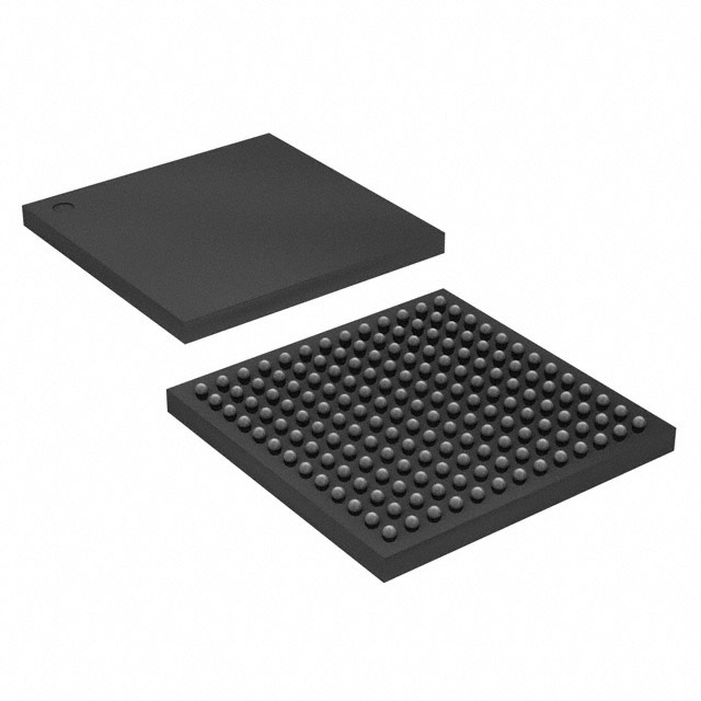
10M16SAU169I7G Package Photo — 169-Ball UBGA (11 mm × 11 mm) Industrial Grade (Source: Manufacturer Photo)
2. Specifications and Parameter Table
| Parameter | Value |
|---|---|
| Manufacturer | Intel (formerly Altera) |
| Device Family | MAX 10 (Non-Volatile FPGA) |
| Logic Elements (LEs) | 16,000 |
| Logic Array Blocks (LABs) | 1,000 |
| Embedded Memory (M9K) | 549 Kb (66 M9K blocks) |
| Embedded 18×18 Multipliers | 45 |
| Phase-Locked Loops (PLLs) | 4 |
| User I/O Pins (U169) | 130 |
| Maximum LVDS Pairs | 22 |
| Analog-to-Digital Converter | Dual 12-bit SAR ADC, up to 1 MSPS |
| User Flash Memory (UFM) | Yes (on-chip non-volatile storage) |
| Configuration Storage | Internal Flash (dual boot supported) |
| External Memory Interface | DDR3, DDR2, LPDDR2, SRAM |
| I/O Standards | 3.3 V / 2.5 V / 1.8 V / 1.5 V / 1.2 V LVCMOS, LVTTL, SSTL, HSTL, LVDS |
| Core Voltage | 1.2 V |
| I/O Supply Voltage | 2.85 V to 3.465 V |
| Process Technology | 55 nm (TSMC embedded flash) |
| Speed Grade | 7 |
| Package | UBGA-169 (11 mm × 11 mm), 0.8 mm pitch |
| Operating Temperature | −40°C to +100°C (Industrial) |
| RoHS Compliance | RoHS Compliant, Lead-Free |
Looking for 10M16SAU169I7G Inventory?
Check our real-time stock levels, pricing, and volume discounts for global distribution.
Check 10M16SAU169I7G Stock3. Architecture, Pinout, and Application Circuit
The MAX 10 architecture centers around a sea of adaptive logic modules (ALMs) simplified into logic elements, each containing a four-input look-up table (LUT), a programmable register, and carry chain logic. The 1,000 LABs in the 10M16 are interconnected via a multi-track routing fabric that provides deterministic timing for high-frequency designs. The four PLLs, each with five output counters, support clock frequencies from 5 MHz to 472.5 MHz with advanced features including clock switchover, phase shifting in 45-degree increments, and spread-spectrum clocking for EMI reduction.
The 10M16SAU169I7G in the U169 package provides 130 user I/O pins organized into multiple I/O banks, each independently configurable for different voltage standards. The dual ADC blocks share a common analog input mux with up to 18 channels, supporting single-ended inputs with programmable sequencing, averaging, and threshold-based event triggering. The ADCs can operate in normal mode, temperature sensing mode, or a combined mode for simultaneous external and die-temperature measurements.
For typical application circuits, Intel recommends separate power supply filtering for the 1.2 V core (VCCINT), 2.5 V PLL analog supply (VCCA), and 3.3 V I/O banks (VCCIO). Each power pin requires a local 0.1 µF ceramic bypass capacitor, with additional 10 µF bulk capacitors per supply rail. The configuration flash supports dual-boot images, enabling remote firmware updates with automatic fallback to a known-good configuration if the primary image fails.
10M16SAU169I7G Typical Application Circuit — Power Supply, Clock, and I/O Interface Design (Source: Intel/Altera Reference Design)
4. Video: Intel MAX 10 FPGA Tutorial
This video provides an overview of Intel MAX 10 FPGA features including instant-on configuration, integrated ADC, user flash memory, and development with Quartus Prime. The MAX 10 family is ideal for bridging, I/O expansion, and sensor processing applications where non-volatile single-chip integration reduces board complexity and BOM cost.
5. Equivalents, Cross-Reference, and Lifecycle
The 10M16SAU169I7G is part of Intel’s actively manufactured MAX 10 product line. Within the MAX 10 10M16 sub-family, several package and temperature variants are available for cross-reference:
- 10M16SAU169C8G – Commercial temperature (0°C to +85°C), speed grade 8, same U169 package. Suitable for consumer and commercial applications not requiring extended temperature range.
- 10M16SAE144C8G – Commercial grade in 144-pin EQFP package. Offers 102 user I/Os with easier prototyping due to larger pin pitch.
- 10M16SCU169I7G – Industrial grade, U169 package, with analog and flash features. Similar to the SA variant with different feature set configuration.
- 10M16DAF484I7G – Industrial grade in 484-ball FBGA package, providing up to 320 user I/Os for designs requiring maximum connectivity.
For designers considering migration to newer architectures, Intel’s Cyclone 10 LP family offers pin-compatible and function-compatible options with higher logic density, while the Cyclone V SE family provides an integrated ARM Cortex-A9 hard processor system. The MAX 10 family remains in active production with no end-of-life notices as of 2026.
Need Help Selecting the Right FPGA?
Our team can assist with cross-reference, lifecycle analysis, and sourcing for Intel MAX 10 FPGAs.
Contact Us for a Quote6. Frequently Asked Questions (FAQ)
Q1: What is the difference between the 10M16SAU169I7G and the 10M16SAU169C8G?
The primary differences are temperature range and speed grade. The 10M16SAU169I7G is an industrial-grade device rated for −40°C to +100°C with speed grade 7, while the 10M16SAU169C8G is a commercial-grade device rated for 0°C to +85°C with speed grade 8. The “I” suffix denotes industrial temperature, and the “C” suffix denotes commercial. Despite the higher speed grade number on the C8G variant, the I7G is specifically characterized and tested for reliable operation across a wider temperature range, making it the preferred choice for outdoor, automotive-adjacent, and harsh industrial environments.
Q2: Does the 10M16SAU169I7G require an external configuration memory?
No. The MAX 10 FPGA family features internal configuration flash memory, which stores the FPGA bitstream on-chip. This eliminates the need for an external EEPROM or flash configuration device, reducing BOM cost and board space. The 10M16SAU169I7G supports dual configuration images, enabling remote firmware updates with automatic fallback to a golden image if the primary configuration fails to load. Configuration time from power-on is typically less than 10 ms.
Q3: What development tools are needed to program the 10M16SAU169I7G?
The 10M16SAU169I7G is fully supported by Intel Quartus Prime Lite Edition, which is available as a free download. Quartus Prime provides design entry (Verilog, VHDL, schematic), synthesis, place-and-route, timing analysis, and programming. For on-chip debugging, Intel provides the Signal Tap Logic Analyzer and In-System Memory Content Editor. Programming is performed via JTAG using an Intel USB-Blaster or USB-Blaster II download cable. The MAX 10 is also supported in the Quartus Prime Standard Edition for customers requiring advanced features.
Q4: How do I use the integrated ADC in the 10M16SAU169I7G?
The dual 12-bit SAR ADCs are instantiated using the Quartus Prime IP Catalog’s “Modular ADC Core” IP block. Each ADC supports up to 1 MSPS sampling rate with up to 18 multiplexed analog input channels. The ADC IP provides configurable sequencing (single-channel, round-robin, or custom sequence), hardware averaging (up to 256 samples), and threshold-based interrupt generation. The analog input voltage range is 0 V to the VREFP reference (typically 2.5 V or 3.3 V). An on-die temperature sensor channel is also available for thermal monitoring without consuming external analog pins.
Q5: Can the 10M16SAU169I7G interface with DDR3 SDRAM?
Yes. The MAX 10 10M16 device supports DDR3, DDR2, and LPDDR2 external memory interfaces through its hard memory controller IP. In the U169 package, the available I/O count (130 pins) limits the memory interface width, but a x8 or x16 DDR3 interface is achievable depending on remaining I/O budget. The UniPHY-based memory controller handles DQS alignment, read/write leveling, and calibration automatically. For wider memory interfaces or higher bandwidth requirements, consider the 10M16DAF484 variant with 320 user I/Os.
Q6: What is the User Flash Memory (UFM) and how is it used?
The User Flash Memory (UFM) is a dedicated block of non-volatile flash memory separate from the configuration flash. It allows designers to store application-specific data such as calibration coefficients, serial numbers, encryption keys, or boot parameters that persist across power cycles. The UFM is accessed through the Quartus Prime “On-Chip Flash” IP core, which provides a simple Avalon Memory-Mapped interface for read and write operations from the FPGA fabric. Write operations are sector-based and require an erase cycle before programming. The UFM supports at least 20,000 program/erase cycles with 20-year data retention.
Related Products on wwdparts.com


