
Request a Quote · 10M16SAU169I7G
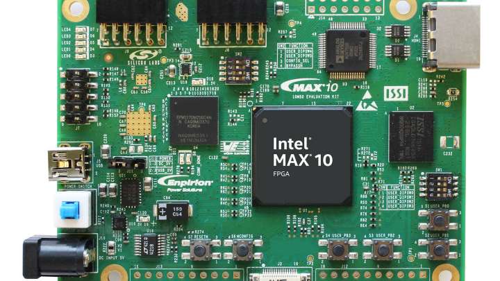
Intel MAX 10 FPGA Architecture Overview — Logic Array Blocks, Embedded Memory, PLLs, ADC, and I/O Structure (Source: Intel/Altera)
The 10M16SAU169I7G is a non-volatile FPGA from Intel’s (formerly Altera) MAX 10 family, integrating 16,000 logic elements, 549 Kb of embedded SRAM, 45 embedded 18×18 multipliers, and a dual-channel analog-to-digital converter—all within a compact 169-ball UBGA package measuring just 11×11 mm. Built on TSMC’s 55 nm flash process technology with integrated configuration flash, the 10M16SAU169I7G eliminates the need for external configuration memory and achieves instant-on operation. Rated for the industrial temperature range (−40°C to +100°C), it delivers reliable performance for system management, I/O expansion, motor control, sensor aggregation, and protocol bridging applications.
Table of Contents
1. Overview and Core Features
The MAX 10 family represents Intel’s single-chip, non-volatile FPGA platform, combining the flexibility of programmable logic with the simplicity of instant-on configuration storage. The 10M16SAU169I7G sits in the mid-range of the MAX 10 lineup, providing 16,000 logic elements organized in 1,000 logic array blocks (LABs), each containing 16 adaptive logic modules (ALMs). This density is sufficient for implementing complex state machines, multi-channel communication controllers, and signal processing pipelines without requiring external configuration flash or boot ROM.
Key differentiators of the 10M16SAU169I7G include its integrated dual-channel ADC with up to 1 MSPS conversion rate and 12-bit resolution, enabling direct analog sensor interfacing without external ADC ICs. The device features 4 PLLs for flexible clock management, supporting clock multiplication, division, and phase shifting. With 549 Kb of embedded memory configurable as RAM, ROM, shift registers, or FIFO buffers, and 45 embedded 18×18 multipliers for DSP operations, the 10M16SAU169I7G handles mixed-signal and compute-intensive workloads in a single device. The U169 package variant provides 130 user I/O pins with support for 3.3 V LVTTL, LVCMOS, SSTL, HSTL, and LVDS differential signaling standards.
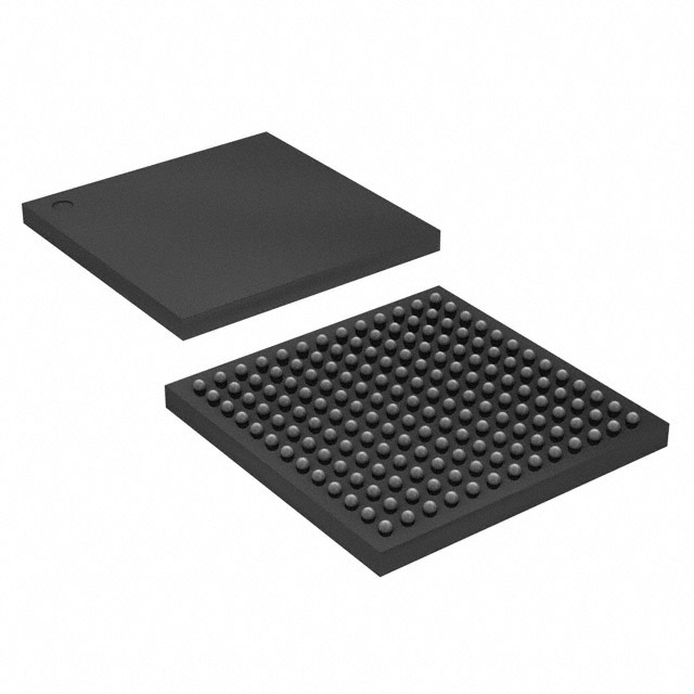
10M16SAU169I7G Package Photo — 169-Ball UBGA (11 mm × 11 mm), Industrial Grade (Source: Microchip USA)
2. Specifications and Parameter Table
| Parameter | Value |
|---|---|
| Manufacturer | Intel (formerly Altera) |
| Family | MAX 10 (Non-Volatile FPGA) |
| Logic Elements (LEs) | 16,000 |
| Logic Array Blocks (LABs) | 1,000 |
| Embedded Memory | 549 Kb (562,176 bits) — M9K blocks |
| Embedded 18×18 Multipliers | 45 |
| PLLs | 4 |
| User I/O Pins | 130 (U169 package) |
| Analog-to-Digital Converter | Dual-channel, 12-bit, up to 1 MSPS |
| User Flash Memory | Yes (integrated on-chip) |
| Configuration Storage | Internal flash (instant-on, no external config device) |
| Core Voltage (VCC) | 1.2 V |
| I/O Voltage (VCCIO) | 2.85 V to 3.465 V |
| I/O Standards | 3.3 V LVTTL, 1.0–3.3 V LVCMOS, SSTL, HSTL, LVDS, LVPECL |
| Speed Grade | 7 (Industrial) |
| Operating Temperature | −40°C to +100°C (TJ) |
| Process Technology | 55 nm (TSMC) |
| Package | 169-UBGA (11 mm × 11 mm), 0.8 mm pitch |
| External Memory Interface | DDR2, DDR3, LPDDR2, SRAM |
| RoHS Compliance | RoHS Compliant |
| Product Status | Active |
Looking for 10M16SAU169I7G Inventory?
Check our real-time stock levels, pricing, and volume discounts for global distribution.
Check 10M16SAU169I7G Stock3. Architecture, Pinout, and Application Circuit
The 10M16SAU169I7G implements the MAX 10 non-volatile FPGA architecture where the device fabric is organized around a grid of LABs interconnected by a high-performance routing network. Each LAB contains 16 logic elements with dedicated carry chains and register packing capability. The embedded memory consists of M9K blocks (9,216 bits each including parity), which can be configured as single-port RAM, dual-port RAM, ROM, or FIFO with data widths from ×1 to ×36. The 45 embedded 18×18 multipliers support signed and unsigned multiplication with optional input/output register pipelining, enabling efficient implementation of FIR/IIR filters and MAC operations.
The U169 package provides 130 user I/O pins distributed across multiple I/O banks, each independently configurable for different voltage standards. The device supports JTAG-based configuration through the IEEE 1149.1 TAP controller, as well as internal configuration from on-chip flash with optional dual-image support for remote update. The integrated ADC block accepts analog inputs from dedicated analog pins and delivers 12-bit conversion results accessible via the Avalon memory-mapped interface in NIOS II soft processor or custom logic designs.
For typical applications, Intel recommends decoupling each VCC pin with 0.1 µF and 10 µF capacitors, along with proper ground plane design for the BGA footprint. The JTAG pins (TCK, TMS, TDI, TDO) should include pull-up or pull-down resistors per the Intel configuration guidelines. The MAX 10 Development Kit provides a reference design with Gigabit Ethernet, HDMI, and HSMC interfaces for rapid prototyping.

Intel MAX 10 FPGA Development Kit — Reference Platform with Gigabit Ethernet, HDMI, USB-UART, and HSMC Expansion (Source: Altera/Intel)
4. Video: MAX 10 FPGA Development Tutorial
This tutorial covers the fundamentals of developing with Intel MAX 10 FPGAs, including Quartus Prime project setup, pin assignment, device programming via JTAG, and leveraging the integrated ADC and flash memory features unique to the MAX 10 family.
5. Equivalents, Cross-Reference, and Lifecycle
The 10M16SAU169I7G is an active product in Intel’s current portfolio. Within the MAX 10 family, closely related variants include the 10M16SAU169C8G (commercial temperature, speed grade 8), the 10M16SAU169A7G (automotive temperature rating), and the 10M08SAU169I7G (8K LE variant in the same U169 package for cost-optimized designs). For applications requiring more logic density, the 10M25SAE144C8G (25K LEs in E144 package) offers a pin-compatible upgrade path within the MAX 10 ecosystem.
Compared to competing non-volatile FPGA platforms, the MAX 10 family competes with Lattice MachXO3 and Microchip PolarFire devices. The MAX 10’s key advantage is its integrated ADC and dual-image flash configuration capability, while Lattice MachXO3 offers lower static power consumption for battery-powered applications. Designers migrating from Altera MAX V CPLDs will find the MAX 10 a natural upgrade path with significantly more logic resources and embedded features.
6. Frequently Asked Questions (FAQ)
What is the difference between 10M16SAU169I7G and 10M16SAU169C8G?
The 10M16SAU169I7G is the industrial-grade variant rated for −40°C to +100°C junction temperature with speed grade 7, while the 10M16SAU169C8G is the commercial-grade variant rated for 0°C to +85°C with speed grade 8. Despite the higher speed grade number, the “I7G” suffix indicates slower timing (industrial screening) compared to the “C8G” commercial part. Choose the I7G for applications requiring extended temperature reliability such as industrial automation, outdoor deployments, or automotive-adjacent systems.
Does the 10M16SAU169I7G require an external configuration flash?
No. The MAX 10 family integrates on-chip configuration flash memory, eliminating the need for external serial configuration devices (such as EPCS or EPCQ). The device supports single-image and dual-image configuration modes, with the dual-image mode enabling remote field updates with a safe fallback image. This instant-on capability means the FPGA is operational within milliseconds of power-up, with no external boot sequence required.
How do I use the integrated ADC in the 10M16SAU169I7G?
The MAX 10 integrated ADC is accessed via the Altera Modular ADC IP core in Quartus Prime. The dual-channel 12-bit SAR ADC supports up to 1 MSPS and can be connected to dedicated analog input pins. In Quartus Prime, instantiate the ADC core via the IP Catalog, configure the number of channels and sequencing mode, and connect it to your design via the Avalon memory-mapped interface. The ADC supports both single-ended and temperature-sensing modes. Note that not all U169 package pins support analog input—refer to the device pinout file for dedicated analog pin assignments.
What development tools are needed for the 10M16SAU169I7G?
The 10M16SAU169I7G is supported by Quartus Prime Lite Edition, which is free to download from Intel’s website. This includes the full synthesis, place-and-route, timing analysis, and programming toolchain. For hardware programming, you need a USB-Blaster or USB-Blaster II JTAG cable. Popular development boards like the Terasic DE10-Lite and Arrow MAX1000 feature MAX 10 devices with on-board USB-Blaster circuits. The Quartus Prime software also includes the NIOS II Embedded Design Suite for soft processor implementation and the Platform Designer (Qsys) for system integration.
Can the 10M16SAU169I7G interface with DDR3 SDRAM?
Yes, the MAX 10 family supports DDR3 SDRAM via its External Memory Interface (EMIF) IP core. The device includes dedicated DQS/DQ pin groups optimized for DDR timing requirements. However, the U169 package has limited pin count (130 I/O), which may restrict the DDR3 data width. For wider DDR3 interfaces, consider the larger U324 or F484 package variants of the 10M16. The EMIF IP core in Quartus Prime handles PHY calibration, timing, and leveling automatically. DDR2 SDRAM and LPDDR2 are also supported as lower-power alternatives.
What is the power consumption of the 10M16SAU169I7G?
Static power consumption for the 10M16SAU169I7G is typically in the range of 90–150 mW depending on junction temperature and I/O configuration. Dynamic power depends heavily on the design’s logic utilization, toggle rates, and clock frequencies. Intel provides the Early Power Estimator (EPE) spreadsheet and the PowerPlay Power Analyzer tool within Quartus Prime for accurate power estimation at different design stages. For low-power designs, the MAX 10 supports programmable I/O standards that minimize I/O switching power, and unused I/O banks can be powered down.
Need Help Sourcing 10M16SAU169I7G?
wwdparts.com offers competitive pricing, fast global shipping, and technical support for Intel FPGA components.
Get a Quote Now Browse All ComponentsRelated Components: 10M16SAU169C8G 10M08SAE144C8G EP4CE10E22C8N


