
10M16SAU169I7G: Datasheet, Pinout, Block Diagram & Application Guide | Intel MAX 10 FPGA
The 10M16SAU169I7G is an industrial-grade, non-volatile FPGA from Intel’s (formerly Altera) MAX 10 family, built on TSMC’s 55 nm embedded flash process. It packs 16,000 logic elements, 549 Kbit of M9K embedded SRAM, 45 hardware 18×18-bit multipliers, dual on-die configuration flash images, a 12-bit 1 MSPS SAR ADC with dedicated analog channels, and 4 PLLs — all inside a compact 169-pin UBGA package measuring 11×11 mm. With an extended industrial temperature range of −40 °C to +100 °C, single 3.3 V supply operation, and instant-on boot under 10 ms, the 10M16SAU169I7G is purpose-built for harsh-environment applications in industrial automation, communications infrastructure, defense systems, and field instrumentation.
1. Overview and Part Number Decoding
The 10M16SAU169I7G belongs to Intel’s MAX 10 FPGA product line, which combines non-volatile instant-on capability with true FPGA flexibility. Unlike traditional FPGAs that require external configuration flash, the MAX 10 stores up to two configuration images in on-chip user flash memory (UFM), enabling power-on in under 10 ms with no external boot ROM.
Breaking down the ordering code 10M16SAU169I7G:
- 10M — MAX 10 FPGA family
- 16 — 16,000 logic elements
- SA — Single-supply, analog feature set (integrated ADC)
- U169 — 169-ball UBGA package (11×11 mm)
- I7 — Industrial temperature (−40 °C to +100 °C), speed grade 7
- G — Lead-free / RoHS-compliant packaging
The “I7” suffix is critical for designs destined for factory floors, outdoor enclosures, or under-hood automotive environments where commercial-grade (0 °C to +85 °C) devices would be inadequate. Speed grade 7 is the standard performance tier in the MAX 10 family, suitable for clocking up to approximately 300 MHz in optimized datapaths.
2. Specifications and Parameter Table
| Parameter | Value |
|---|---|
| Manufacturer | Intel (formerly Altera) |
| Family | MAX 10 (10M) |
| Logic Elements (LEs) | 16,000 |
| Logic Array Blocks (LABs) | 1,000 |
| Embedded SRAM (M9K) | 549 Kbit (61 M9K blocks) |
| User Flash Memory (UFM) | 2,368 Kbit |
| 18×18 Multipliers | 45 |
| PLLs | 4 |
| Max User I/O | 130 (in U169 package) |
| Max LVDS Pairs | 22 |
| ADC | Dual 12-bit SAR, up to 1 MSPS, up to 18 channels |
| External Memory Interfaces | DDR3, DDR2, LPDDR2, SRAM |
| Supply Voltage (VCC) | 3.0 V – 3.3 V (single supply) |
| I/O Voltage | 1.2 V, 1.5 V, 1.8 V, 2.5 V, 3.3 V (multi-bank) |
| Speed Grade | 7 |
| Temperature Range | −40 °C to +100 °C (Industrial) |
| Package | 169-ball UBGA (11 × 11 mm, 0.8 mm pitch) |
| Process Node | 55 nm (TSMC embedded flash) |
| Configuration | Internal flash (dual image, instant-on <10 ms) |
| I/O Standards | 3.3 V LVTTL, LVCMOS, SSTL, HSTL, LVDS, RSDS, Mini-LVDS, LVPECL |
| RoHS | Yes (Pb-free) |
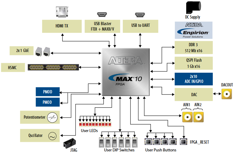
3. Architecture and Block Diagram
The MAX 10 architecture revolves around a sea of adaptive logic modules (ALMs) organized into LABs, each containing 16 logic elements with dedicated carry chains and register packing. Surrounding the logic fabric are hardened resources: M9K SRAM blocks (each 9,216 bits configurable as single- or dual-port RAM, ROM, or FIFO), 18×18 hardware multipliers for DSP-intensive workloads, and 4 general-purpose PLLs offering up to 5 output clocks each with frequency synthesis from 100 kHz to 472.5 MHz.
A defining feature is the on-chip analog-to-digital converter — a dual-core 12-bit successive-approximation register (SAR) ADC capable of 1 MSPS aggregate throughput. This eliminates external ADC components in mixed-signal designs such as temperature monitoring, voltage rail supervision, or sensor fusion. The ADC is accessed through a soft IP core instantiated in Quartus Prime, providing Avalon-MM bus connectivity to Nios II or custom logic.
Dual configuration flash images enable fail-safe remote update: the factory image is protected while a new application image is programmed over JTAG or through user logic. If the new image fails CRC, the device automatically reverts to the factory configuration — critical for deployed industrial equipment.
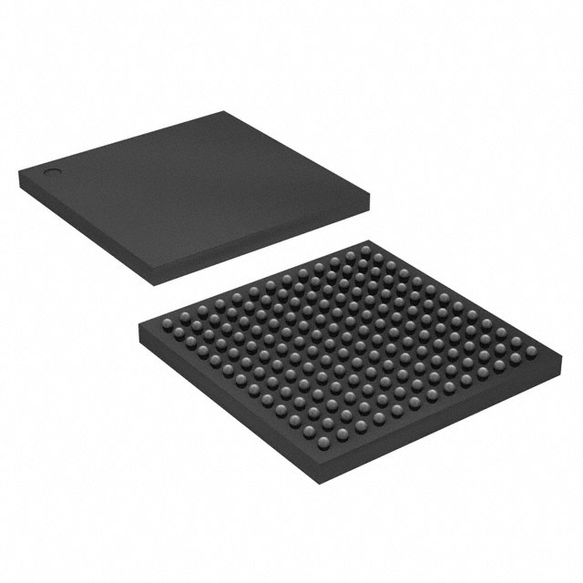
4. Pinout and Package Details
The 10M16SAU169I7G is housed in a 169-ball UBGA package with a 13×13 ball array at 0.8 mm pitch, yielding an 11×11 mm body. Of the 169 balls, 130 are user I/O organized across 8 I/O banks with independent VCCIO supplies, enabling simultaneous multi-voltage interfacing (e.g., 3.3 V LVTTL on one bank, 1.8 V LVCMOS on another).
Key pin assignments include:
- JTAG pins (TDI, TDO, TMS, TCK) — dedicated programming and boundary-scan interface
- nSTATUS, nCONFIG, CONF_DONE — configuration status and control signals
- CLK inputs — dedicated clock input pins routed to PLL clock networks
- ADC analog input pins — dedicated pins for analog-to-digital conversion channels
- VCC, VCCIO, GND — core supply (1.2 V internal), I/O bank supplies, and ground planes
For production layout, Intel recommends a 4-layer PCB stack-up minimum with dedicated ground and power planes. BGA fanout uses dog-bone vias at the 0.8 mm pitch, with via-in-pad plated over (VIPPO) for high-density routing. Decoupling capacitors (100 nF ceramic) should be placed within 2 mm of each VCC and VCCIO ball.
5. Application Circuits and Design Tips
The 10M16SAU169I7G excels in applications demanding non-volatile, instant-on FPGA logic with mixed-signal capability in harsh environments:
- Industrial motor control — PWM generation, encoder interface, and current sensing via the integrated ADC, all in a single chip
- Communications protocol bridging — converting between SPI, I2C, UART, and custom serial protocols with deterministic timing
- Sensor fusion nodes — aggregating multiple analog sensor channels through the ADC while performing digital filtering in fabric
- Edge computing gateways — implementing lightweight ML inference accelerators with the 45 multipliers providing up to 900 MMAC/s at 300 MHz
- Test and measurement instruments — data acquisition front-ends with the ADC and DDR3 buffer memory
Design tips for the 10M16SAU169I7G:
- Power sequencing — VCCINT (1.2 V core) must ramp before VCCIO. Use Intel’s power calculator spreadsheet to size the regulator for worst-case dynamic current.
- Thermal management — At +100 °C ambient, ensure adequate copper pour and airflow. The UBGA thermal resistance (θJA) is approximately 25 °C/W; high-utilization designs may need a heatsink.
- ADC reference — Route the ADC VREF with a star topology and decouple with a 1 μF ceramic + 10 μF tantalum close to the pin for best INL/DNL.
- Clock planning — Each of the 4 PLLs can multiply and divide the input clock. Use regional clock networks to minimize skew across I/O banks.
Video Tutorial: Getting Started with MAX 10 FPGA
6. FAQ
The “I7” suffix denotes industrial temperature range (−40 °C to +100 °C) with speed grade 7, while the “C8” suffix indicates commercial temperature range (0 °C to +85 °C) with speed grade 8. The I7G variant is screened and guaranteed to operate reliably in extreme thermal environments, making it essential for outdoor, automotive, and heavy-industry deployments. Speed grade 8 is slightly faster; however, the industrial screening of the I7G ensures consistent timing margins across its wider temperature range.
No. The MAX 10 family integrates on-chip configuration flash memory that stores up to two full configuration images internally. The device self-configures from internal flash at power-up in under 10 ms, eliminating the BOM cost and board space of an external SPI flash. This also improves reliability by reducing solder joints and potential failure points.
Instantiate the “Modular ADC Core” IP in Intel Quartus Prime via the Platform Designer (formerly Qsys) tool. The IP provides an Avalon-MM slave interface that connects to a Nios II processor or custom state machine. Configure the channel sequencer to scan your desired analog input pins, set the sampling rate (up to 1 MSPS aggregate), and read conversion results from the data registers. For best analog performance, route the ADCVREF pin with a star topology and decouple with low-ESR capacitors close to the device.
Intel Quartus Prime Lite Edition (free) fully supports all MAX 10 devices. The design flow includes synthesis, place-and-route, timing analysis (TimeQuest), simulation with ModelSim-Intel Starter Edition, and programming via USB-Blaster or USB-Blaster II. Third-party synthesis tools like Synopsys Synplify Pro are also compatible. For schematic symbols and PCB footprints, check SnapEDA or Ultra Librarian for verified packages.
Yes. The MAX 10 includes a hard memory controller supporting DDR3, DDR2, and LPDDR2 SDRAM at up to 300 MHz (DDR3-600). In the U169 package, a subset of I/O banks supports the necessary SSTL-15 signaling. Use Intel’s External Memory Interface (EMIF) Toolkit in Quartus Prime to configure the controller, generate calibration logic, and verify signal integrity with the board-aware timing model.
Within the MAX 10 family, the 10M16SAU169C8G (commercial temp) is pin-compatible if industrial temperature is not required. For higher density, the 10M25SAU169I7G (25K LEs) shares the same U169 pinout. Cross-family alternatives include the Lattice MachXO3LF-6900 (similar density, non-volatile) and the Microchip PolarFire MPF100 (for higher performance needs). Always verify I/O voltage compatibility and pinout mapping when cross-referencing.
Related components available at WWDParts:


