
Request a Quote · 10M16SAU169I7G
Intel MAX 10 FPGA Architecture Block Diagram — Logic Array Blocks, Embedded Memory, PLLs, ADC, and User Flash Memory (Source: Intel/Altera)
The 10M16SAU169I7G is a non-volatile FPGA from Intel’s (formerly Altera) MAX 10 family, fabricated on a 55 nm process node. Featuring 16,000 logic elements, 549 Kb of embedded memory, 45 embedded 18×18 multipliers, an integrated dual analog-to-digital converter, and user flash memory, this device delivers instant-on functionality in a compact 169-ball UBGA package. With an industrial temperature range of −40°C to +100°C and support for single-chip, single-power-supply operation at 3.3 V, the 10M16SAU169I7G is purpose-built for cost-sensitive industrial, automotive, and embedded control applications that require FPGA flexibility without external configuration flash.
Table of Contents
1. Overview and Core Features
The Intel MAX 10 family represents the industry’s first single-chip, non-volatile FPGA with integrated dual-configuration flash. The 10M16SAU169I7G occupies the mid-range of this family, offering 16,000 logic elements organized into 1,000 logic array blocks (LABs), each containing 16 adaptive logic modules (ALMs). This provides ample resources for implementing complex digital logic, state machines, soft-core processors, and custom peripherals—all without the need for an external configuration memory device.
A standout feature of the MAX 10 is its integrated analog-to-digital converter. The 10M16SAU169I7G includes a dual 12-bit SAR ADC (ADC1 and ADC2), each capable of up to 1 MSPS conversion rate with up to 18 analog input channels. This enables direct sensor interfacing without external analog front-end components, reducing BOM cost and board area. The device also provides up to 736 Kb of user flash memory (UFM) for in-system non-volatile data storage such as calibration constants, serial numbers, and firmware.
With 4 PLLs providing flexible clock synthesis and management, 130 user I/O pins supporting LVTTL, LVCMOS (1.2 V to 3.3 V), and differential LVDS standards, and DDR2/DDR3/LPDDR2 external memory interfaces, the 10M16SAU169I7G delivers a complete system-on-chip solution for applications including motor drives, sensor hubs, industrial IoT gateways, and communications infrastructure.

MAX 10 FPGA UBGA-169 Package (11 mm × 11 mm) — 169-Ball Ultra FineLine BGA, 0.8 mm Ball Pitch (Source: Microchip USA)
2. Specifications and Parameter Table
| Parameter | Value |
|---|---|
| Manufacturer | Intel / Altera |
| Family | MAX 10 (Non-Volatile FPGA) |
| Logic Elements (LEs) | 16,000 |
| Logic Array Blocks (LABs) | 1,000 |
| Embedded Memory | 549 Kb (M9K blocks) |
| Embedded 18×18 Multipliers | 45 |
| Phase-Locked Loops (PLLs) | 4 |
| User I/O Pins | 130 (UBGA-169 package) |
| Maximum LVDS Pairs | 22 |
| Analog-to-Digital Converter | Dual 12-bit SAR ADC, up to 1 MSPS |
| User Flash Memory (UFM) | Up to 736 Kb |
| External Memory Support | DDR2, DDR3, LPDDR2, SRAM |
| I/O Standards | 3.3 V / 2.5 V / 1.8 V / 1.5 V / 1.2 V LVCMOS/LVTTL, LVDS, SSTL |
| Core Voltage | 1.2 V |
| I/O Supply Voltage | 1.2 V to 3.3 V |
| Process Technology | 55 nm |
| Speed Grade | 7 (Slowest) |
| Package | UBGA-169 (11 mm × 11 mm, 0.8 mm pitch) |
| Operating Temperature | −40°C to +100°C (Industrial) |
| Configuration | Internal dual-boot flash (instant-on) |
| Bitstream Security | AES-128 encryption supported |
| RoHS Compliance | RoHS Compliant |
Looking for 10M16SAU169I7G Inventory?
Check our real-time stock levels, pricing, and volume discounts for global distribution.
Check 10M16SAU169I7G Stock3. Architecture, Pinout, and Application Circuit
The MAX 10 architecture centers on a sea of logic array blocks (LABs) surrounded by I/O elements, embedded memory blocks, DSP blocks, and clock networks. Each LAB contains 16 logic elements, where each LE includes a 4-input look-up table (LUT), a programmable register, and carry chain logic for efficient arithmetic operations. The 45 embedded 18×18 multipliers enable hardware-accelerated DSP functions such as FIR/IIR filtering and FFT computation without consuming general logic resources.
The 10M16SAU169I7G in its UBGA-169 package provides 130 user I/O pins arranged across 8 I/O banks. Each bank can be independently powered at different voltage levels (1.2 V to 3.3 V), allowing seamless interfacing with mixed-voltage systems. The device supports up to 22 LVDS differential pairs for high-speed serial links and offers dedicated pins for JTAG configuration, analog inputs, and clock inputs.
For a typical application circuit, the MAX 10 requires a 1.2 V core supply (VCCINT), a 2.5 V analog supply (VCCA), and per-bank I/O supplies. Intel recommends 0.1 µF and 10 µF decoupling capacitors on each power pin, with all unused I/O pins configured as inputs with internal pull-up resistors enabled. The dual-configuration flash supports a factory image plus an application image, enabling remote firmware updates with safe fallback—a critical feature for field-deployed industrial systems.
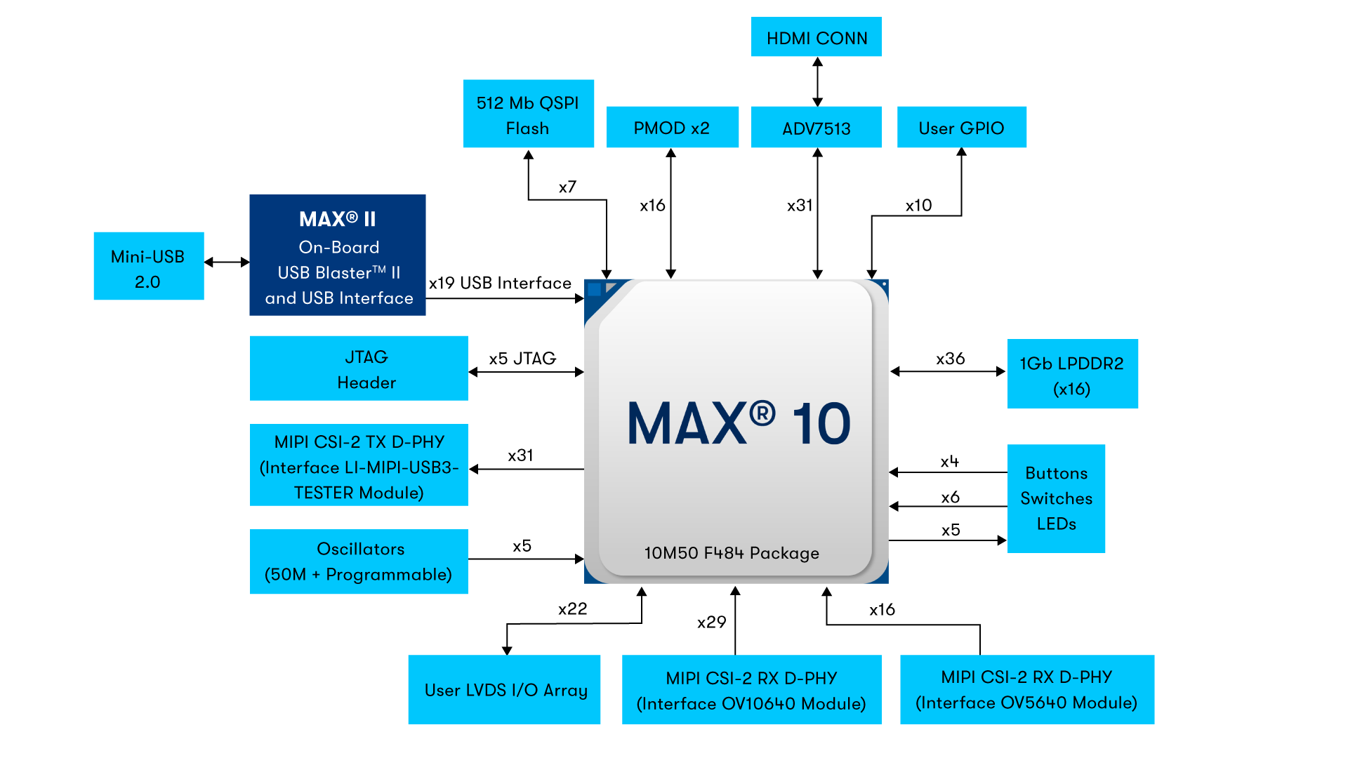
MAX 10 FPGA 10M50 Evaluation Kit Block Diagram — DDR3, ADC, HDMI, MIPI CSI-2, and Pmod Interfaces (Source: Intel/Altera)
4. Video: MAX 10 FPGA Development
This video covers getting started with Intel MAX 10 FPGA development using Quartus Prime software. Topics include device configuration, pin assignment, logic design, and programming the evaluation board—directly applicable to designs using the 10M16SAU169I7G.
5. Equivalents, Cross-Reference, and Lifecycle
The 10M16SAU169I7G carries an Active production status from Intel/Altera. The “I7G” suffix indicates the industrial temperature grade (−40°C to +100°C) with speed grade 7. For designs requiring different specifications or alternative devices, engineers should consider:
- 10M16SAU169C8G — Same 16K LE device in UBGA-169 but with commercial temperature range (0°C to +85°C) and faster speed grade 8. A direct pin-compatible swap when industrial temperature is not required.
- 10M08SAU169C8G — Lower-density variant with 8,000 logic elements in the same UBGA-169 package. Pin-compatible and cost-optimized for designs that need fewer logic resources.
- 10M25SAE144C8G — Higher-density 25K LE MAX 10 device in a 144-pin EQFP package. Suitable for designs requiring more logic and I/O resources with through-hole prototyping capability.
- Lattice MachXO3LF-6900C — A competing non-volatile FPGA from Lattice Semiconductor offering approximately 6,900 LUTs with integrated flash and instant-on operation. An alternative when vendor diversification is needed.
When migrating between MAX 10 variants, pin migration is supported across devices sharing the same package footprint. Use Intel’s Pin Migration Viewer in Quartus Prime to verify I/O compatibility. Check 10M16SAU169I7G Inventory & Pricing at WWDParts for current lead times and stock availability.
6. Frequently Asked Questions (FAQ)
Q1: What is the 10M16SAU169I7G, and what applications is it designed for?
The 10M16SAU169I7G is a non-volatile FPGA from Intel’s MAX 10 family featuring 16,000 logic elements, integrated dual ADC, and on-chip configuration flash in a 169-ball UBGA package. It is designed for industrial control systems, motor drives, sensor aggregation hubs, building automation, automotive infotainment, communications infrastructure, and any application requiring instant-on FPGA functionality with industrial-grade temperature tolerance (−40°C to +100°C).
Q2: What is the difference between the 10M16SAU169I7G and 10M16SAU169C8G?
Both devices share the same 16,000 LE core and UBGA-169 package. The key differences are: the I7G variant operates over the industrial temperature range (−40°C to +100°C) with speed grade 7, while the C8G variant covers the commercial range (0°C to +85°C) with the faster speed grade 8. Choose the I7G for harsh environment deployments and the C8G for cost-optimized designs operating within controlled temperature conditions.
Q3: Does the 10M16SAU169I7G require an external configuration flash memory?
No. The MAX 10 family integrates on-chip configuration flash memory, enabling instant-on operation without any external configuration device. The 10M16SAU169I7G supports dual-configuration images, allowing a factory safe image and an application image for remote field updates with automatic fallback if the application image fails to load.
Q4: How many analog input channels does the integrated ADC support?
The 10M16SAU169I7G includes a dual 12-bit SAR ADC block (ADC1 and ADC2). The total number of available analog input channels depends on the pin configuration, with up to 18 channels available across both ADC blocks. Each ADC can achieve a sampling rate of up to 1 MSPS with 12-bit resolution, suitable for temperature monitoring, voltage sensing, and basic data acquisition tasks.
Q5: What development tools and software are needed to program the 10M16SAU169I7G?
Intel’s Quartus Prime Lite Edition (free, no license required) fully supports the MAX 10 family including the 10M16SAU169I7G. The toolchain includes schematic capture, Verilog/VHDL synthesis, place-and-route, timing analysis (TimeQuest), and the built-in programmer for JTAG configuration. For system-level integration, Intel provides the Platform Designer (formerly Qsys) tool for building Nios II soft-processor systems with peripherals.
Q6: Can I use the 10M16SAU169I7G for DDR3 memory interfaces?
Yes. The 10M16SAU169I7G supports DDR2, DDR3, and LPDDR2 external memory interfaces through its dedicated I/O pins with built-in DQS/DQ alignment circuitry. Intel provides a hardened DDR memory controller IP through Quartus Prime’s IP Catalog. However, when using the UBGA-169 package, the available I/O count (130 pins) may limit the DDR3 data bus width; consult the Intel MAX 10 Pin-Out Files to verify available memory interface pins for this specific package.


