
Request a Quote · 10M16SAU169I7G

MAX 10 FPGA Architecture Block Diagram — Logic Array Blocks, Embedded Memory, PLLs, ADC, and User I/O (Source: Altera/Intel)
The 10M16SAU169I7G is a non-volatile FPGA from the Intel (Altera) MAX 10 family, built on 55 nm flash process technology. Featuring 16,000 logic elements, 549 Kb of embedded memory, four PLLs, and an integrated 12-bit ADC, this device delivers instant-on functionality with dual configuration flash in a compact 169-ball UBGA package. The industrial-grade temperature rating (−40°C to +100°C) and speed grade 7 make it well suited for factory automation, motor control, sensor aggregation, and cost-sensitive embedded systems requiring deterministic boot without external configuration memory.
Table of Contents
1. Overview and Core Features
The MAX 10 FPGA family represents Intel (formerly Altera)’s single-chip, non-volatile FPGA solution optimized for cost-sensitive and space-constrained applications. The 10M16SAU169I7G integrates 16,000 logic elements organized into 1,000 Logic Array Blocks (LABs), providing substantial combinational and registered logic capacity. Unlike traditional SRAM-based FPGAs that require external flash memory for configuration, the MAX 10 stores up to two configuration images in its on-chip flash, enabling instant-on operation within milliseconds of power-up.
Key features of the 10M16SAU169I7G include 549 Kb of embedded M9K memory blocks that can be configured as RAM, ROM, FIFO, or shift registers. The four analog PLLs support clock frequencies up to 500 MHz with fractional synthesis, clock switchover, and dynamic reconfiguration. The integrated 12-bit successive-approximation ADC with up to 18 analog input channels eliminates the need for external ADC ICs in sensor-interface designs. For multiply-accumulate operations, the device provides embedded multiplier blocks suitable for basic DSP tasks such as digital filtering and motor control algorithms.
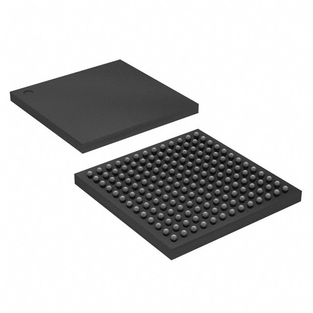
10M16SAU169I7G Package Photo — 169-Ball UBGA (11 mm × 11 mm) Industrial Grade (Source: MicrochipUSA)
2. Specifications and Parameter Table
| Parameter | Value |
|---|---|
| Manufacturer | Intel (formerly Altera) |
| Family | MAX 10 (10M16) |
| Device Type | Non-Volatile FPGA |
| Logic Elements (LEs) | 16,000 |
| Logic Array Blocks (LABs) | 1,000 |
| Embedded Memory (M9K) | 549 Kb (62 M9K blocks) |
| User Flash Memory (UFM) | 128 Kb |
| PLLs | 4 (analog, up to 500 MHz) |
| Embedded Multipliers (18×18) | 45 |
| ADC | 12-bit SAR, up to 1 MSPS, 18 channels |
| User I/O Pins (U169 package) | 130 |
| LVDS Pairs | 22 |
| I/O Standards | 3.3 V / 2.5 V / 1.8 V / 1.5 V LVCMOS, LVTTL, SSTL, HSTL, LVDS |
| External Memory Interface | DDR3, DDR3L, DDR2, LPDDR2 |
| Core Voltage | 1.2 V |
| I/O Supply Voltage | 1.5 V / 1.8 V / 2.5 V / 3.0 V / 3.3 V (bank-selectable) |
| Speed Grade | 7 (lowest power) |
| Operating Temperature | −40°C to +100°C (Industrial) |
| Process Technology | 55 nm Flash |
| Package | 169-Ball UBGA (U169), 11 mm × 11 mm |
| Configuration | Dual boot from internal flash (instant-on) |
| Bitstream Security | AES-128 encryption |
| RoHS Compliance | RoHS Compliant, Lead-Free |
Looking for 10M16SAU169I7G Inventory?
Check our real-time stock levels, pricing, and volume discounts for global distribution.
Check 10M16SAU169I7G Stock3. Architecture, Pinout, and Application Circuit
The MAX 10 architecture organizes logic resources into a two-dimensional array of LABs, each containing 16 adaptive logic modules (ALMs) with look-up tables and registers. M9K embedded memory blocks (9,216 bits each) are distributed throughout the fabric for low-latency local storage. The four analog PLLs are positioned at device corners, each providing five output counters with independent phase shift, duty cycle, and frequency division. I/O pins are grouped into eight banks with independent voltage supply, supporting simultaneous operation of multiple I/O standards.
The integrated 12-bit ADC operates at up to 1 MSPS with a dedicated analog reference block and multiplexed input channels. This ADC connects to the FPGA fabric through an Avalon-MM interface, enabling software-triggered or hardware-triggered conversions. The on-chip flash stores configuration data and up to 128 Kb of user flash memory (UFM), accessible at runtime for data logging, calibration coefficients, or secure key storage. Dual configuration flash supports remote field updates with automatic fallback to a known-good image.
In the U169 package, the 10M16SAU169I7G provides 130 user I/O pins distributed across eight I/O banks. The pinout supports up to 22 LVDS transmitter/receiver pairs for high-speed board-to-board signaling. For a typical application, the device interfaces with DDR3 memory, SPI flash for additional storage, and various sensor peripherals through GPIO and LVDS, while the integrated ADC handles analog sensor inputs directly.

MAX 10 FPGA Development Kit — Evaluation Board with DDR3, Gigabit Ethernet, HDMI, ADC, and JTAG (Source: Altera)
4. Video: MAX 10 FPGA Tutorial
This tutorial covers the Intel MAX 10 FPGA platform, including Quartus Prime project setup, pin assignment, device programming via JTAG, and leveraging the integrated ADC and flash memory. The content is directly applicable to designs using the 10M16SAU169I7G and other MAX 10 family devices.
5. Equivalents, Cross-Reference, and Lifecycle
The 10M16SAU169I7G carries an Active production status from Intel/Altera. The MAX 10 family was introduced in 2014 and continues to receive long-term support. For designs requiring alternative specifications or second-source options, consider the following:
- 10M16SAU169C8G — Same 10M16 device in U169 package with commercial temperature range (0°C to +85°C) and speed grade 8. A lower-cost option when industrial temperature range is not required.
- 10M16SAE144I7G — The 10M16 in a 144-pin EQFP package with industrial temperature rating. Offers more I/O pins (102) in a larger QFP form factor that simplifies hand soldering and prototyping.
- 10M08SAU169I7G — A smaller MAX 10 device with 8,000 logic elements in the same U169 package and industrial temperature grade. Suitable when the design fits within 8K LEs for lower cost.
- 10M25SAU169I7G — A larger MAX 10 device with 25,000 logic elements in the same U169 package, for designs that need additional logic capacity while maintaining the same footprint.
- Lattice MachXO3LF-6900C — A non-volatile FPGA alternative from Lattice Semiconductor with similar instant-on capability and comparable logic density, for multi-vendor sourcing strategies.
When selecting an alternative, verify that the I/O count, memory resources, and PLLs meet your design requirements. Check 10M16SAU169I7G Inventory & Pricing at WWDParts for current lead times and stock availability.
6. Frequently Asked Questions (FAQ)
Q1: What is the 10M16SAU169I7G, and what applications is it designed for?
The 10M16SAU169I7G is a non-volatile FPGA from Intel’s MAX 10 family, featuring 16,000 logic elements, 549 Kb embedded memory, four PLLs, and an integrated 12-bit ADC in a 169-ball UBGA package with industrial temperature rating (−40°C to +100°C). It is designed for applications requiring instant-on operation without external configuration memory, including industrial automation, motor control, sensor aggregation, LED signaling, communications protocol bridging, and cost-sensitive embedded systems. The integrated ADC makes it particularly well suited for mixed-signal designs that combine analog sensing with digital processing.
Q2: How does the MAX 10 instant-on dual boot configuration work?
The MAX 10 FPGA stores up to two complete configuration images in its internal flash memory. Upon power-up, the device automatically loads the selected image and configures itself within approximately 2 ms, without requiring any external configuration memory or processor intervention. The dual-boot capability supports remote field updates: a new image is written to the secondary flash sector, verified, and then set as the primary boot image. If the new image fails to load, the device automatically falls back to the previous known-good image, ensuring system reliability during firmware upgrades.
Q3: What are the key differences between the U169 and E144 packages for the 10M16?
The U169 package is a 169-ball UBGA measuring 11 mm × 11 mm, providing 130 user I/O pins and up to 22 LVDS pairs. The E144 package is a 144-pin EQFP measuring 22 mm × 22 mm, offering 102 user I/O pins. The U169 has a significantly smaller footprint (about 4× less board area) and supports more I/Os, making it preferable for space-constrained, high-density designs. The E144 is easier to hand-solder and inspect, making it better suited for prototyping and low-volume production. Both packages share the same silicon die and feature set.
Q4: How do I use the integrated ADC on the 10M16SAU169I7G?
The MAX 10 ADC is a 12-bit successive-approximation converter operating at up to 1 MSPS with up to 18 multiplexed analog input channels. In Quartus Prime, instantiate the ADC IP core using the Platform Designer (Qsys) tool, which generates an Avalon-MM slave interface for register-level access. The ADC supports software-triggered single conversions and hardware-triggered continuous scanning. Analog inputs accept 0 V to the VREFH reference voltage (typically 2.5 V or 3.3 V). External anti-aliasing RC filters on each analog input are recommended, and the dedicated ANAIN pins should be routed away from high-speed digital traces to minimize noise coupling.
Q5: What external power supply design is recommended for the 10M16SAU169I7G?
The device requires a 1.2 V core supply (VCCINT), one or more I/O bank supplies (VCCIO) selectable from 1.5 V, 1.8 V, 2.5 V, or 3.3 V, and a 2.5 V analog supply (VCCA) for the PLLs and ADC. Each supply rail should have 0.1 µF and 10 µF decoupling capacitors placed close to the BGA pads. Intel recommends a specific power-up sequence: VCCINT first, followed by VCCIO, then VCCA. A power-on reset circuit should hold nCONFIG low until all supplies are stable. For the U169 package, the central ground pad must be connected to the PCB ground plane through multiple vias for proper thermal and electrical performance.
Q6: Can the 10M16SAU169I7G interface with DDR3 memory, and what is the maximum supported data rate?
Yes. The MAX 10 FPGA supports DDR3, DDR3L, DDR2, and LPDDR2 external memory interfaces through dedicated hard memory controller IP. In the U169 package, the available I/O pins support a single x16 DDR3 interface operating at up to 300 MHz (600 Mbps per pin). Use the External Memory Interface Toolkit in Quartus Prime to configure the memory controller, generate timing constraints, and calibrate the interface. The memory controller handles refresh, read/write leveling, and on-chip termination automatically. For industrial temperature designs, derate the maximum frequency based on the speed grade 7 timing specifications in the datasheet.
For more FPGA and programmable logic options, browse our MAX 10 FPGA catalog or explore our full semiconductor inventory. See also our guide on the latest FPGA technology trends.
Alan Carter, Senior Hardware Engineer
Alan has over 15 years of experience in FPGA design and embedded systems, specializing in Intel/Altera programmable logic, mixed-signal integration, and global semiconductor supply chain management.


