
10M16SAU169I7G Datasheet, Specifications & Pinout – Altera MAX 10 FPGA
The 10M16SAU169I7G is a high-performance MAX 10 FPGA from Altera (now Intel PSG), featuring 16,000 logic elements in a compact 169-ball UBGA package. Built on 55 nm non-volatile process technology, this industrial-grade FPGA integrates embedded flash memory, analog-to-digital converters, and phase-locked loops for single-chip system solutions. It is widely used in industrial automation, motor control, sensor hubs, and IoT edge computing.
Overview & Key Features
The 10M16SAU169I7G belongs to the Intel (Altera) MAX 10 FPGA family, a product line that uniquely combines non-volatile FPGA fabric with user flash memory and dual analog-to-digital converters on a single die. Unlike traditional FPGAs that require external configuration memory, the MAX 10 stores its configuration internally, enabling instant-on operation at power-up.
- 16,000 logic elements (1,000 LABs) for versatile digital logic
- 549 Kb embedded SRAM for data buffering and FIFO
- Dual ADC blocks with up to 18 analog input channels and 12-bit resolution
- 4 PLLs for flexible clock synthesis and management
- Instant-on with internal configuration flash – no external EEPROM needed
- User flash memory up to 736 Kb for storing application data
- Industrial temperature range (−40 °C to +100 °C)
Specifications & Electrical Parameters
| Parameter | Value |
|---|---|
| Part Number | 10M16SAU169I7G |
| Family | MAX 10 (Intel / Altera) |
| Logic Elements (LEs) | 16,000 |
| Logic Array Blocks (LABs) | 1,000 |
| Embedded Memory (SRAM) | 549 Kb (562,176 bits) |
| User Flash Memory (UFM) | 736 Kb |
| 18×18 Multipliers | 45 |
| PLLs | 4 |
| ADC Blocks | 1 dual-ADC block (12-bit, up to 1 MSPS) |
| Maximum User I/O (U169) | 130 |
| Maximum LVDS Pairs | 22 |
| Package | UBGA-169 (11 × 11 mm) |
| Core Voltage (VCCINT) | 1.2 V (1.15–1.25 V) |
| I/O Voltage | 1.2 V – 3.3 V |
| Process Technology | 55 nm (non-volatile) |
| Speed Grade | 7 (industrial) |
| Temperature Range | −40 °C to +100 °C |
| External Memory Support | DDR3, DDR2, LPDDR2, SRAM |
| I/O Standards | LVTTL, LVCMOS, SSTL, HSTL, PCI, LVDS |
| Configuration | Internal flash (instant-on), JTAG |
| RoHS | Compliant |
Block Diagram & Architecture
The MAX 10 architecture integrates programmable logic, embedded memory, DSP multiplier blocks, PLLs, ADC, user flash, and a flexible I/O ring on a single die. The logic fabric is organized into logic array blocks (LABs), each containing 10 adaptive logic modules (ALMs) with look-up tables and registers.

Key architectural highlights include the non-volatile configuration scheme that allows dual boot images, enabling safe remote firmware updates with a factory fallback image.
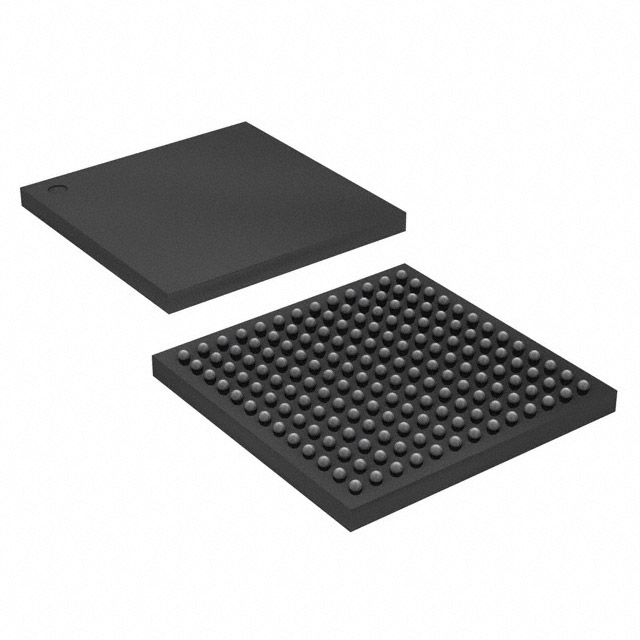
Pinout & Package Information
The 10M16SAU169I7G is housed in a 169-ball UBGA (Ultra Fine-pitch Ball Grid Array) package with an 11 × 11 mm body size and 0.8 mm ball pitch. It provides 130 user I/O pins organized across multiple I/O banks supporting voltage levels from 1.2 V to 3.3 V.
The I/O banks support a wide range of single-ended and differential standards including LVDS, SSTL, and HSTL, making the device compatible with popular memory interfaces and high-speed signaling.
Application Circuit & Design Tips
The MAX 10 FPGA Development Kit provides a reference design platform featuring dual Gigabit Ethernet, HDMI output, DDR3 memory, and analog front-end connections. The 10M16SAU169I7G is commonly used in:
- Industrial sensor fusion and motor control
- LED signage and display controllers
- Automotive infotainment pre-processing
- IoT edge gateways and protocol bridges
- Test and measurement equipment

Getting Started – Video Tutorial
FAQ – 10M16SAU169I7G
What is the 10M16SAU169I7G?
The 10M16SAU169I7G is an Altera (Intel) MAX 10 FPGA with 16,000 logic elements, integrated dual ADC, and non-volatile flash configuration in a 169-ball UBGA package. It supports an industrial temperature range of −40 °C to +100 °C.
What is the package type of the 10M16SAU169I7G?
The 10M16SAU169I7G uses a UBGA-169 (Ultra Fine-pitch Ball Grid Array) package with an 11 × 11 mm body size and 0.8 mm ball pitch, providing 130 user I/O pins.
Does the 10M16SAU169I7G have an integrated ADC?
Yes. The 10M16SAU169I7G includes a dual analog-to-digital converter (ADC) block with 12-bit resolution and up to 1 MSPS sampling rate, supporting up to 18 analog input channels for direct sensor interfacing.
What software tools are used to program the 10M16SAU169I7G?
The 10M16SAU169I7G is programmed using Intel Quartus Prime Lite Edition (free), which supports Verilog, VHDL, and schematic design entry. Configuration is done via JTAG or the internal flash memory.
What is the difference between 10M16SAU169I7G and 10M16SAU169C8G?
Both share the same logic resources and package (UBGA-169). The "I7" suffix denotes industrial temperature range (−40 °C to +100 °C) and speed grade 7, while "C8" denotes commercial temperature range (0 °C to +85 °C) and speed grade 8.
Where can I buy the 10M16SAU169I7G?
The 10M16SAU169I7G is available from authorized distributors including wwdparts.com, DigiKey, Mouser, Arrow, and Octopart. Always verify stock availability and lead times before placing orders.


