
Request a Quote · 10M16SAU169I7G

10M16SAU169I7G UBGA-169 Package and Pinout Reference
The 10M16SAU169I7G is a non-volatile FPGA from Intel (formerly Altera), belonging to the MAX 10 device family. Built on a 55 nm flash process, this device integrates 16,000 logic elements, embedded SRAM, user flash memory, PLLs, DSP blocks, and an analog-to-digital converter (ADC) into a compact 169-pin UBGA package. It targets industrial-grade applications with an extended operating temperature range of −40°C to +100°C and a speed grade of 7 (slowest). The MAX 10 family is notable for eliminating the need for an external configuration device, reducing both BOM cost and board area in space-constrained designs.
Table of Contents
1. Overview and Core Features
The Intel MAX 10 FPGA family was introduced to bridge the gap between CPLDs and low-density FPGAs. The 10M16SAU169I7G sits in the mid-range of this family, offering 16,000 logic elements (LEs) organized into 1,000 logic array blocks (LABs). Each LAB contains 16 LEs, and each LE provides a four-input look-up table (LUT), a programmable register, and carry chain logic.
Key differentiators of this device include:
- Dual configuration flash: On-chip flash stores two configuration images, supporting remote system upgrade without an external EPROM or SPI flash.
- Integrated ADC: A 12-bit, 1 MSPS SAR ADC with up to 18 analog input channels enables direct sensor interfacing, eliminating external ADC ICs.
- User flash memory (UFM): Up to 736 Kb of non-volatile storage available for application data, serial numbers, or calibration constants.
- Instant-on: Configuration from internal flash completes in less than 10 ms, suitable for applications requiring fast power-on readiness.
- Industrial temperature: The I7G suffix indicates −40°C to +100°C operation, appropriate for factory automation, transportation, and outdoor equipment.
2. Specifications and Parameter Table
| Parameter | Value |
|---|---|
| Part Number | 10M16SAU169I7G |
| Manufacturer | Intel (Altera) |
| Family | MAX 10 (10M16) |
| Logic Elements (LEs) | 16,000 |
| Logic Array Blocks (LABs) | 1,000 |
| Embedded Memory (M9K Blocks) | 549 Kb (562,176 bits) |
| User Flash Memory (UFM) | Up to 736 Kb |
| 18×18 Embedded Multipliers | 45 |
| PLLs | 4 |
| Maximum User I/O | 130 |
| Analog-to-Digital Converter | 12-bit SAR ADC, 1 MSPS |
| Package | UBGA-169 (11 mm × 11 mm) |
| I/O Standards | 3.3 V / 2.5 V / 1.8 V / 1.5 V LVCMOS, LVDS, SSTL, HSTL, PCI |
| Core Voltage | 1.2 V |
| Operating Temperature | −40°C to +100°C (Industrial) |
| Speed Grade | 7 (Slowest) |
| Process Technology | 55 nm Flash |
| Configuration | Internal (dual-boot, instant-on) |
| External Memory Interface | DDR3, DDR2, LPDDR2, SRAM |
| RoHS Compliant | Yes (Lead-Free, “G” suffix) |
Looking for 10M16SAU169I7G Inventory?
Check our real-time stock levels, pricing, and volume discounts for global distribution.
Check 10M16SAU169I7G Stock3. Architecture and Block Diagram
The MAX 10 architecture organizes logic resources in a column-based floorplan. LAB columns are interleaved with M9K embedded memory columns and DSP (embedded multiplier) columns. I/O banks surround the logic core, each independently configurable for different voltage standards. The diagram below illustrates the functional block layout of the MAX 10 FPGA family.
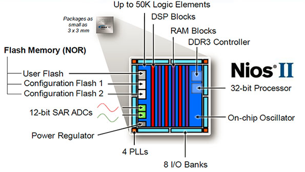
MAX 10 FPGA Architecture Block Diagram
The on-chip ADC block connects to a dedicated analog input bank, supporting both single-ended and differential input modes. The four PLLs, distributed at the device corners, generate clock frequencies from 0 MHz to 500 MHz with jitter under 200 ps. Each PLL includes five output counters, enabling complex clocking topologies without external oscillator ICs.

10M16SAU169I7G Schematic Symbol Reference
4. Video: MAX 10 FPGA Development Kit Tutorial
5. Equivalents, Cross-Reference, and Lifecycle
The 10M16SAU169I7G remains in active production as of 2026. Intel (Altera) continues to support the MAX 10 family through the Quartus Prime Lite Edition (free license). When evaluating pin-compatible or functionally equivalent alternatives within the MAX 10 lineup, consider the following variants:
- 10M16SAU169C8G – Same device in commercial temperature (0°C to +85°C) with speed grade 8. Suitable when industrial temperature is not required.
- 10M08SAU169C8G – Lower-density variant (8,000 LEs) in the same U169 package. Pin-compatible for designs that can fit in fewer logic resources.
- 10M25SAU169I7G – Higher-density option (25,000 LEs) in U169 package for designs requiring additional logic headroom.
For migration to newer Intel FPGA families, the Cyclone 10 LP series offers a similar cost profile with higher logic density, though it requires external configuration storage. The Lattice MachXO3 family competes in the same non-volatile FPGA segment.
6. Frequently Asked Questions (FAQ)
What is the 10M16SAU169I7G?
The 10M16SAU169I7G is a non-volatile FPGA from Intel's MAX 10 family. It integrates 16,000 logic elements, 549 Kb of embedded memory, a 12-bit ADC, and dual-boot flash configuration in a 169-pin UBGA package. The “I7G” suffix indicates industrial temperature range (−40°C to +100°C), speed grade 7, and lead-free (RoHS) packaging.
Does the 10M16SAU169I7G require an external configuration device?
No. The MAX 10 family stores its configuration bitstream in on-chip flash memory, eliminating the need for an external EPROM or SPI flash IC. This reduces BOM cost and simplifies PCB layout. The device supports dual-image storage for remote field upgrades.
What design software supports the 10M16SAU169I7G?
Intel Quartus Prime Lite Edition (free, no license required) fully supports all MAX 10 devices. It includes synthesis, place-and-route, timing analysis, the Platform Designer (formerly Qsys) system integration tool, and the Signal Tap II logic analyzer for on-chip debugging.
What is the difference between speed grade 7 and speed grade 8 in MAX 10?
Speed grade 7 is the slowest timing grade, while speed grade 8 is faster. A lower speed grade number in Intel FPGAs indicates slower propagation delays. The 10M16SAU169I7G (grade 7) is typically paired with the industrial temperature range, while grade-8 parts like the 10M16SAU169C8G target commercial temperature applications.
What are typical applications for the 10M16SAU169I7G?
Common applications include industrial motor control, sensor aggregation hubs, protocol bridging (SPI/I2C/UART), LED display controllers, power supply sequencing, and small-scale signal processing. The integrated ADC makes it well-suited for mixed-signal systems where direct sensor digitization replaces discrete ADC ICs.
Can the 10M16SAU169I7G interface with DDR3 SDRAM?
Yes. The MAX 10 family includes a hard memory controller IP that supports DDR3, DDR2, and LPDDR2 external memory interfaces. The 10M16 in the U169 package provides sufficient I/O pins for a 16-bit DDR3 interface, enabling frame buffers, data logging, or software-defined processing with external RAM.
Alan Carter, Senior Hardware Engineer
Alan has over 15 years of experience in embedded systems design, specializing in ARM Cortex architectures, PCB routing for high-speed digital signals, and industrial IoT deployments. He frequently contributes technical teardowns and architecture comparisons.


