
The 10M16SAU169I7G is a high-performance, low-cost FPGA from the Altera (Intel) MAX 10 family. Built on 55nm non-volatile technology, this single-chip programmable logic device integrates flash memory, analog-to-digital converters, and rich I/O capabilities into a compact 169-pin UBGA package. It is widely used in industrial automation, motor control, communications, and consumer electronics applications where instant-on operation and low system cost are critical.
Overview & Key Features
The 10M16SAU169I7G belongs to Intel's MAX 10 FPGA product line, which was designed to deliver the lowest system cost and power in a single-chip FPGA solution. Unlike traditional FPGAs that require external configuration memory, the MAX 10 family features dual on-chip configuration flash, enabling instant-on functionality and remote field upgrades. This makes the 10M16SAU169I7G an ideal choice for applications requiring fast boot times and high reliability.
Key features of the 10M16SAU169I7G include:
- 16,000 Logic Elements (LEs) – sufficient for mid-complexity digital designs
- Integrated ADC – up to 2 ADC blocks with 12-bit resolution at 1 MSPS, eliminating the need for external ADC ICs
- 549 Kb Embedded Memory – M9K memory blocks configurable as RAM, ROM, or FIFO
- 4 PLLs – flexible clocking with frequency synthesis and phase shifting
- User Flash Memory (UFM) – non-volatile storage for user data and system parameters
- Industrial Temperature Range – operates from -40°C to +100°C
- DDR3/DDR2/LPDDR2 Memory Interface Support
For purchasing and stock availability, visit the wwdparts.com components catalog.
Technical Specifications
| Parameter | Value |
|---|---|
| Part Number | 10M16SAU169I7G |
| Manufacturer | Altera (Intel) |
| Family | MAX 10 FPGA |
| Logic Elements (LEs) | 16,000 |
| Logic Array Blocks (LABs) | 1,000 |
| Embedded Memory | 549 Kb (M9K blocks) |
| Total RAM Bits | 562,176 |
| Embedded 18×18 Multipliers | 45 |
| PLLs | 4 |
| Maximum User I/O Pins | 130 (U169 package) |
| Maximum LVDS Pairs | 22 |
| Analog-to-Digital Converter | 1 ADC block, 12-bit, 1 MSPS |
| User Flash Memory (UFM) | 2,880 Kb |
| Configuration Flash Memory (CFM) | Dual boot capable |
| Supply Voltage (VCC) | 1.2V (core), 3.3V (I/O) |
| I/O Standards | 3.3V/2.5V/1.8V/1.5V LVCMOS/LVTTL, SSTL, HSTL, LVDS |
| External Memory Interface | DDR3, DDR2, LPDDR2 |
| Operating Temperature | -40°C to +100°C (Industrial) |
| Speed Grade | 7 (lowest speed) |
| Package | UBGA-169 (11 × 11 mm) |
| Process Technology | 55 nm |
| RoHS Compliance | Yes (Lead-Free, "G" suffix) |
Need help choosing the right FPGA for your project? Browse our FPGA collection at wwdparts for competitive pricing and fast shipping.
Block Diagram & Architecture
The MAX 10 FPGA architecture is organized around a fabric of Logic Array Blocks (LABs), each containing 16 Logic Elements. The device integrates embedded memory (M9K blocks), DSP-capable 18×18 multipliers, PLLs, a 12-bit ADC, and dual configuration flash memory. The instant-on feature is enabled by internal flash-based configuration, meaning the FPGA is operational within milliseconds of power-up — no external EEPROM or configuration controller is needed.
The MAX 10 device floorplan places I/O banks on all four edges, with the ADC block located at a dedicated position. PLLs are placed at corner positions for optimal clock distribution. The embedded memory and multiplier columns run vertically through the logic fabric, providing short interconnect paths for high-performance DSP and memory-intensive designs.
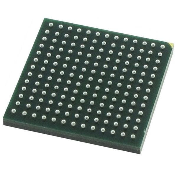
Pinout & Package Information
The 10M16SAU169I7G uses the UBGA-169 package with a 11 × 11 mm body size and 0.8 mm ball pitch. The 169-ball array provides 130 user I/O pins organized into multiple I/O banks, each supporting independent voltage levels. Pin assignments and bank planning can be performed using Intel Quartus Prime software and the official Altera Pin-Out Files.
Key package characteristics:
- Package Type: Ultra Fine-pitch Ball Grid Array (UBGA)
- Pin Count: 169 balls
- Body Size: 11 mm × 11 mm
- Ball Pitch: 0.8 mm
- Height: 1.0 mm max
- Moisture Sensitivity Level: MSL-3
Application Circuit & Design Resources
The 10M16SAU169I7G is well-suited for a broad range of embedded and industrial applications, including:
- Industrial Automation – Motor control, sensor hub, PLC co-processor
- Communications – Protocol bridging, interface conversion, small-cell baseband
- Automotive – ADAS preprocessing, LED control, CAN/LIN gateway
- Consumer Electronics – Video processing, display timing, USB/I2C/SPI bridge
- IoT & Edge Computing – Sensor fusion, data aggregation, real-time control
The official MAX 10 FPGA Development Kit from Altera provides a complete hardware platform to evaluate and prototype designs using MAX 10 devices:

The development kit features dual Gigabit Ethernet, HDMI output, USB-to-UART, HSMC expansion, and analog inputs for ADC evaluation. Design entry is done using Intel Quartus Prime Lite Edition (free), which supports Verilog, VHDL, and schematic capture for MAX 10 devices. Check out our semiconductor technology blog for more FPGA design tutorials and component guides.
Video Tutorial: Getting Started with MAX 10 FPGA
Frequently Asked Questions
What is the 10M16SAU169I7G?
The 10M16SAU169I7G is an Altera (Intel) MAX 10 FPGA with 16,000 logic elements, integrated ADC, and dual configuration flash memory in a 169-pin UBGA package. It is designed for cost-sensitive industrial and embedded applications that require instant-on operation.
What is the operating temperature range of the 10M16SAU169I7G?
The 10M16SAU169I7G is rated for the industrial temperature range of -40°C to +100°C, as indicated by the "I" suffix in the part number. This makes it suitable for harsh operating environments in automotive, industrial, and outdoor applications.
Does the 10M16SAU169I7G require external configuration memory?
No. The MAX 10 FPGA family includes on-chip dual configuration flash, which stores the FPGA bitstream internally. This eliminates the need for external EEPROM or flash configuration devices, reducing BOM cost and board space. The device also supports dual-boot for failsafe remote updates.
What software is used to program the 10M16SAU169I7G?
Intel Quartus Prime Lite Edition is the recommended free development tool for MAX 10 FPGAs. It supports design entry (Verilog, VHDL, schematic), synthesis, place-and-route, timing analysis, and device programming via USB-Blaster or USB-Blaster II.
What is the difference between 10M16SAU169I7G and 10M16SAU169C8G?
Both are MAX 10 16K LE devices in the U169 package. The key differences are: the "I7" variant is industrial grade (-40°C to +100°C, speed grade 7), while the "C8" variant is commercial grade (0°C to +85°C, speed grade 8). The industrial variant offers wider temperature operation at a slightly lower maximum clock frequency.
Can the 10M16SAU169I7G interface with DDR3 memory?
Yes. The MAX 10 FPGA family supports DDR3, DDR2, and LPDDR2 external memory interfaces. The 10M16SAU169I7G can drive DDR3 SDRAM at up to 300 MHz (DDR3-600), making it suitable for applications requiring high-bandwidth data buffering or processing.


