
10M16SAU169I7G Datasheet, Specifications & Application Guide | Intel MAX 10 FPGA
Overview of the 10M16SAU169I7G
The 10M16SAU169I7G is a non-volatile FPGA from Intel (formerly Altera) belonging to the MAX 10 family. Built on a 55nm flash process, this device integrates 16,000 logic elements, an analog-to-digital converter (ADC), and dual configuration flash memory into a compact UBGA-169 package. The "I7G" suffix designates the industrial temperature grade (-40°C to +100°C) with speed grade 7, making it suitable for harsh-environment applications such as industrial automation, motor control, and sensor interface designs.
Unlike traditional FPGAs, the MAX 10 family eliminates the need for an external configuration device — the on-chip flash stores the bitstream and allows instant-on operation. This single-chip solution reduces board space, lowers BOM cost, and simplifies system design. The device is supported by Intel Quartus Prime Lite Edition (free), making it accessible for both prototyping and production.
Key Specifications & Parameters
| Parameter | Value |
|---|---|
| Part Number | 10M16SAU169I7G |
| Family | Intel MAX 10 (formerly Altera) |
| Logic Elements (LEs) | 16,000 |
| Logic Array Blocks (LABs) | 1,000 |
| Embedded Memory | 549 Kb (M9K blocks) |
| 18×18 Multipliers | 45 |
| PLLs | 4 |
| Global Clock Networks | 20 |
| User I/O Pins | 130 (U169 package) |
| ADC | 1× 12-bit, up to 1 MSPS |
| Package | UBGA-169 (11 × 11 mm) |
| Process Technology | 55 nm flash |
| Core Voltage | 1.2 V |
| I/O Voltage | 3.0 V / 3.3 V |
| Speed Grade | 7 |
| Temperature Range | -40°C to +100°C (Industrial) |
| Configuration | Internal flash (instant-on, no external PROM needed) |
| External Memory Support | DDR3, DDR2, LPDDR2, SRAM |
| I/O Standards | LVTTL, LVCMOS, SSTL, HSTL, LVDS |
Block Diagram & Internal Architecture
The MAX 10 architecture places the user logic fabric at the center, surrounded by embedded memory blocks (M9K), DSP blocks with 18×18 multipliers, and a flexible I/O ring supporting multiple voltage standards. The integrated ADC block connects to dedicated analog input pins for direct sensor interfacing, while the dual-boot flash allows seamless firmware updates in the field.

Key architectural highlights include four PLLs for flexible clock synthesis, 20 global clock networks for low-skew distribution, and built-in configuration flash that stores up to two design images for remote update capability.
Pinout, Package & Footprint
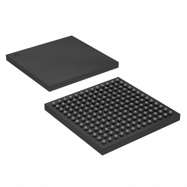
The 10M16SAU169I7G comes in a UBGA-169 (Ultra-Fine-Pitch Ball Grid Array) package measuring 11 × 11 mm with a 0.8 mm ball pitch. This compact form factor delivers 130 user I/O pins across multiple I/O banks, each independently configurable for different voltage standards from 1.2 V to 3.3 V.
When designing your PCB layout, ensure proper decoupling capacitors (100nF ceramic) on each VCC pin and follow Intel's recommended land pattern for the 0.8 mm pitch BGA. The Intel Pin Connection Guidelines document provides detailed pin-by-pin assignment tables and bank grouping information.
Application Circuit & Design Guide
The 10M16SAU169I7G is widely used in applications requiring a compact, low-power FPGA with integrated analog capability:
- Industrial IoT Sensor Hubs: Use the built-in ADC to digitize analog sensor outputs (temperature, pressure, current) and process data locally before transmitting via SPI/I2C/UART.
- Motor Control: Implement PWM generation, encoder interfaces, and closed-loop control algorithms entirely within the FPGA fabric.
- Video & Display Interfaces: Bridge between MIPI, LVDS, and parallel display interfaces with the flexible I/O standards.
- Protocol Bridging: Convert between legacy protocols and modern interfaces (e.g., RS-485 to Ethernet) using Nios II soft processor.
For development and prototyping, Intel offers the MAX 10 FPGA Evaluation Kit which includes USB-Blaster programming, on-board power regulation, and breakout headers for all I/O banks.
Getting Started: Video Tutorial
Frequently Asked Questions
What is the difference between 10M16SAU169I7G and 10M16SAU169C8G?
The main differences are temperature range and speed grade. The I7G variant operates from -40°C to +100°C (industrial) at speed grade 7, while the C8G variant covers 0°C to +85°C (commercial) at speed grade 8. Choose the I7G for applications exposed to wide temperature swings or harsh industrial environments.
Does the 10M16SAU169I7G require an external configuration PROM?
No. The MAX 10 family features internal flash memory for configuration storage. The device boots instantly from its on-chip flash, eliminating the need for an external EEPROM or configuration device. It also supports dual configuration images for safe remote firmware updates.
What software do I need to program the 10M16SAU169I7G?
Use Intel Quartus Prime Lite Edition, which is free and fully supports all MAX 10 devices. It includes the Quartus synthesis/place-and-route tools, ModelSim for simulation, and Platform Designer (formerly Qsys) for system integration. Programming is done via USB-Blaster or USB-Blaster II JTAG cables.
How many user I/O pins are available on the 10M16SAU169I7G?
The UBGA-169 package provides 130 user I/O pins organized into multiple I/O banks. Each bank can be independently set to different voltage standards (1.2V to 3.3V LVCMOS, LVTTL, SSTL, HSTL, or LVDS), giving designers flexibility in interfacing with various peripherals.
Can the 10M16SAU169I7G interface with DDR3 memory?
Yes. The MAX 10 family supports DDR3, DDR2, LPDDR2, and SRAM external memory interfaces. The device includes hard memory controller support for simplified DDR integration, though for complex memory subsystems, larger MAX 10 devices in bigger packages may provide more I/O pins for wider data buses.
What is the power consumption of the 10M16SAU169I7G?
Static power consumption is typically under 150 mW at the industrial temperature maximum. Dynamic power depends on clock frequency, resource utilization, and I/O toggle rates. Intel provides the PowerPlay Early Power Estimator spreadsheet tool to help estimate total power for your specific design before committing to a power supply design.


