
1. Overview of the 10M16SAU169I7G
The 10M16SAU169I7G is a non-volatile FPGA from the Intel (Altera) MAX 10 family, fabricated on a 55 nm process node. It delivers 16,000 logic elements in a compact 169-ball UBGA package, making it an excellent choice for cost-sensitive, single-chip embedded designs. Unlike traditional FPGAs that require an external configuration flash, the MAX 10 integrates dual configuration flash memory on-die, enabling instant-on operation and simplifying the bill of materials.
The device supports an industrial temperature range of –40 °C to +100 °C (speed grade 7) and operates from a 3.3 V core supply (2.85 V–3.465 V). With a built-in 12-bit ADC, 45 embedded 18×18 multipliers, and 4 PLLs, the 10M16SAU169I7G is well-suited for sensor interface, motor control, industrial IoT, and low-power signal-processing applications.
Looking for stock or pricing? Browse the Altera FPGA collection at wwdparts.com for competitive offers on MAX 10 devices.
2. Key Specifications & Parameters
| Parameter | Value |
|---|---|
| Part Number | 10M16SAU169I7G |
| Family | Intel (Altera) MAX 10 |
| Logic Elements (LEs) | 16,000 |
| Logic Array Blocks (LABs) | 1,000 |
| Embedded Memory (M9K) | 549 Kb (562,176 bits) |
| 18 × 18 Multipliers | 45 |
| PLLs | 4 |
| User I/O Pins | 130 |
| ADC | 12-bit, up to 1 MSPS |
| User Flash Memory (UFM) | 2,304 Kb |
| Configuration Flash | Internal (dual image) |
| Package | 169-UBGA (11 × 11 mm) |
| Supply Voltage (VCCINT) | 1.2 V |
| I/O Voltage | 2.85 V – 3.465 V (3.3 V nominal) |
| Temperature Range | –40 °C to +100 °C (Industrial) |
| Speed Grade | 7 |
| Process Node | 55 nm |
| RoHS Status | Compliant (Lead-Free) |
3. Block Diagram & Architecture
The MAX 10 architecture integrates logic array blocks, embedded memory, DSP multipliers, PLLs, a 12-bit ADC, and dual configuration flash into a single monolithic die. The diagram below illustrates the high-level architecture of the Intel MAX 10 FPGA family.
Key architectural highlights include instant-on capability thanks to integrated configuration flash, a flexible I/O bank structure supporting LVTTL, LVCMOS, SSTL, and HSTL standards, and on-chip analog-to-digital conversion eliminating external ADC components.
For detailed pin planning, refer to the wwdparts.com technical blog for more MAX 10 design guides.
4. Pinout & Package Information
The 10M16SAU169I7G uses a 169-ball Ultra-thin Fine-pitch Ball Grid Array (UBGA) measuring 11 × 11 mm with a 0.8 mm ball pitch. This compact form factor is ideal for space-constrained designs in industrial and IoT applications.

The 130 user I/O pins are organized into multiple I/O banks, each independently configurable for different voltage standards. The package supports DDR2, DDR3, and LPDDR2 external memory interfaces for high-bandwidth data paths.
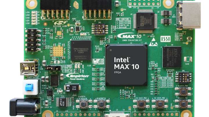
5. Typical Applications & Development Kits
The 10M16SAU169I7G is widely deployed in industrial automation, motor drives, sensor hubs, video bridging, communications infrastructure, and IoT edge computing. Its integrated ADC makes it particularly attractive for mixed-signal applications that previously required a separate analog front-end.

Intel offers the MAX 10 FPGA Development Kit featuring dual Gigabit Ethernet, HDMI output, USB-to-UART, HSMC expansion, and dual ADC SMA inputs—providing a comprehensive platform for prototyping and evaluation.
Need other Intel FPGA parts? Check the Intel FPGA collection at wwdparts.com.
Video Tutorial: Getting Started with MAX 10 FPGA
6. Frequently Asked Questions (FAQ)
Q1: What is the 10M16SAU169I7G?
The 10M16SAU169I7G is a 16,000-logic-element non-volatile FPGA from the Intel (Altera) MAX 10 family. It comes in a 169-UBGA package with 130 user I/Os, an integrated 12-bit ADC, and dual on-chip configuration flash for instant-on operation.
Q2: What is the operating temperature range of the 10M16SAU169I7G?
The 10M16SAU169I7G operates over the industrial temperature range of –40 °C to +100 °C (junction temperature), making it suitable for harsh-environment deployments.
Q3: Does the 10M16SAU169I7G require external configuration memory?
No. The MAX 10 family integrates dual configuration flash on-chip, enabling single-chip instant-on operation without an external EEPROM or flash device.
Q4: How many DSP multipliers does the 10M16SAU169I7G have?
It features 45 embedded 18 × 18 multipliers, suitable for digital signal processing tasks such as filtering, motor control algorithms, and sensor data processing.
Q5: What development tools support the 10M16SAU169I7G?
The device is supported by Intel Quartus Prime Lite Edition (free), which includes synthesis, place-and-route, timing analysis, and the Platform Designer (formerly Qsys) system integration tool. ModelSim Intel FPGA Edition is available for simulation.
Q6: What are common applications for the 10M16SAU169I7G?
Typical applications include industrial automation, motor drives, sensor interface and fusion, communications bridging, IoT edge computing, and mixed-signal systems leveraging the on-chip ADC.


