
Overview of the 10M16SAU169I7G
The 10M16SAU169I7G is a non-volatile FPGA from the Intel (formerly Altera) MAX 10 family, built on a 55 nm flash process. It integrates 16,000 logic elements, an analog-to-digital converter, and up to 296 KB of user flash memory into a compact 169-ball UBGA package. Because configuration data is stored in on-chip flash, the device boots instantly without an external configuration ROM—an advantage that simplifies board design and reduces BOM cost.
The "I7G" suffix denotes the industrial temperature grade (−40 °C to +100 °C) with a speed grade of 7, making the 10M16SAU169I7G suitable for harsh-environment deployments such as industrial automation, motor control, sensor fusion, and field-bus protocol bridging. Designers can program the device with Intel Quartus Prime Lite (free license) using Verilog, VHDL, or schematic entry.
Key Specifications and Parameters
| Parameter | Value |
|---|---|
| Manufacturer | Intel (Altera) |
| Family | MAX 10 (10M16) |
| Logic Elements (LEs) | 16,000 |
| Logic Array Blocks (LABs) | 1,000 |
| Embedded Memory (M9K blocks) | 549 Kb (≈ 61 blocks × 9 Kb) |
| 18 × 18 Multipliers | 45 |
| Phase-Locked Loops (PLLs) | 4 |
| User Flash Memory | Up to 296 KB |
| Analog-to-Digital Converter | Yes – Dual ADC, up to 17 channels, 12-bit, 1 MSPS |
| Maximum User I/O (U169 pkg) | 130 |
| Package | 169-UBGA (11 × 11 mm, 0.8 mm pitch) |
| Supply Voltage (I/O) | 2.85 V – 3.465 V (3.3 V typical) |
| Core Voltage | 1.2 V |
| Operating Temperature | −40 °C to +100 °C (Industrial) |
| Speed Grade | 7 |
| Process Technology | 55 nm Flash |
| External Memory Interface | DDR3, DDR3L, DDR2, LPDDR2 |
| I/O Standards | LVTTL, LVCMOS (1.2–3.3 V), SSTL, HSTL, HSUL, LVDS |
| Configuration | Internal flash (instant-on), dual boot images supported |
| RoHS Compliant | Yes |
Block Diagram and Architecture
The MAX 10 architecture arranges logic array blocks (LABs), M9K embedded memory, DSP multiplier blocks, and PLLs around a central routing fabric. Each LAB contains 10 adaptive logic modules (ALMs) with 4-input look-up tables. The 10M16 variant adds a dual-channel ADC block, user flash memory, and an internal oscillator that supports instant-on configuration without external components.
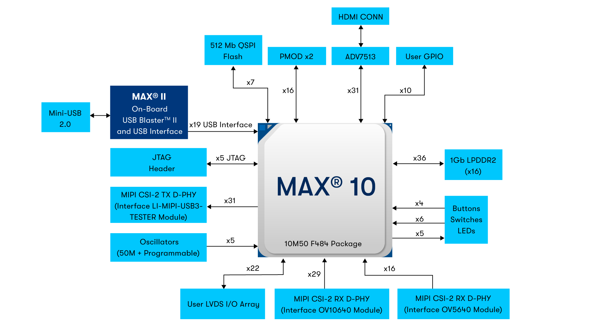
Figure 1 – MAX 10 FPGA evaluation system block diagram illustrating the on-board peripherals, power rails, and FPGA connectivity.
Pinout and Package Information
The 10M16SAU169I7G uses a 169-ball UBGA package measuring 11 × 11 mm with 0.8 mm ball pitch. Of the 169 balls, 130 are available as user I/O, organized across up to 8 I/O banks. Each bank can be independently configured for different voltage standards (1.2 V to 3.3 V). The compact footprint makes the U169 package ideal for space-constrained designs where a high logic-to-board-area ratio is needed.

Figure 2 – Physical package photo of a MAX 10 169-UBGA device, identical form factor to the 10M16SAU169I7G.
Application Circuit and Design Examples
The 10M16SAU169I7G is commonly used in industrial control panels, motor drive interfaces, LED sign controllers, and sensor aggregation hubs. Its built-in ADC eliminates external converters for mixed-signal designs, while the instant-on flash configuration enables rapid startup—critical in safety-rated systems. Engineers can prototype designs on the official MAX 10 FPGA Evaluation Kit, which pairs the MAX 10 FPGA with HDMI, MIPI CSI-2, Pmod, and Ethernet interfaces.

Figure 3 – MAX 10 FPGA Evaluation Board front view, a recommended development platform for 10M16SAU169I7G prototyping.
Video Tutorial: Getting Started with MAX 10 FPGA
Frequently Asked Questions
What is the difference between 10M16SAU169I7G and 10M16SAU169C8G?
The main differences are temperature range and speed grade. The I7G variant is rated for the industrial range (−40 °C to +100 °C) with speed grade 7, while the C8G is commercial (0 °C to +85 °C) with speed grade 8. The I7G is recommended for applications exposed to wide temperature swings.
Does the 10M16SAU169I7G require an external configuration flash?
No. The MAX 10 family stores configuration data in on-chip flash memory, enabling instant-on operation. The device supports dual configuration images for safe remote updates—if the new image fails, it automatically falls back to the factory image.
What software tools are needed to program the 10M16SAU169I7G?
Intel Quartus Prime Lite Edition (free) fully supports MAX 10 devices. It includes synthesis, place-and-route, timing analysis, and the Programmer tool for JTAG configuration. Platform Designer (formerly Qsys) can generate Nios II soft-processor systems for the 10M16.
How many ADC channels does the 10M16SAU169I7G have?
The 10M16 integrates a dual-channel 12-bit ADC with up to 1 MSPS sample rate. Depending on the package and device variant, up to 17 analog input channels are available. The ADC block includes a temperature sensor and internal voltage references.
Can the 10M16SAU169I7G interface with DDR3 memory?
Yes. The MAX 10 hard memory controller IP supports DDR3, DDR3L, DDR2, and LPDDR2 interfaces. For the U169 package with 130 user I/O, the available pin count limits the DDR data bus width, so designers typically use x8 or x16 DDR3 configurations.
Where can I buy the 10M16SAU169I7G?
The 10M16SAU169I7G is available from authorized distributors including wwdparts.com, Digi-Key, Mouser, and Arrow. Check wwdparts.com for competitive pricing, stock availability, and guaranteed authentic parts with full traceability.
Related Components on wwdparts.com
- 10M04SCE144C8G – MAX 10 FPGA (4K LE, E144 Package)
- 10M08SAE144C8G – MAX 10 FPGA (8K LE, E144 Package)
- 10M16SAU169C8G – MAX 10 FPGA (16K LE, U169 Commercial Grade)


