
10M16SAU169I7G Datasheet, Specifications & Application Guide – Altera MAX 10 FPGA
The 10M16SAU169I7G is a non-volatile FPGA from the Altera (Intel) MAX 10 family, built on a 55 nm process node. With 16,000 logic elements, an integrated dual 12-bit ADC, and internal flash configuration memory, this device delivers instant-on capability without requiring an external configuration chip. It is widely adopted in industrial control, IoT edge gateways, motor drives, and sensor-fusion applications where low power, compact packaging, and fast boot times are critical.
1. 10M16SAU169I7G Overview & Part Number Decoder
The 10M16SAU169I7G belongs to the MAX 10 FPGA family, Altera's single-chip, non-volatile FPGA platform. The part number encodes the device's key characteristics:
- 10M16 – MAX 10 family, 16,000 logic elements
- S – Single power-supply mode (simplifies board design)
- A – Analog block enabled (dual 12-bit ADC)
- U169 – 169-ball Ultra Thin Ball Grid Array (UBGA) package
- I – Industrial temperature range (−40 °C to +100 °C)
- 7 – Speed grade 7 (highest performance tier for this device)
Unlike traditional FPGAs that require external flash or EEPROM for configuration, the MAX 10 integrates up to two configuration images in on-die flash, enabling instant-on operation in under 10 ms. This is a game-changer for applications that cannot tolerate long boot sequences, such as safety-critical industrial systems and FPGA-based control modules.
2. Key Specifications & Electrical Parameters
| Parameter | Value |
|---|---|
| Part Number | 10M16SAU169I7G |
| Family | Intel (Altera) MAX 10 |
| Process Node | 55 nm |
| Logic Elements (LEs) | 16,000 |
| Embedded Memory (M9K RAM) | 549 Kb |
| User Flash Memory (UFM) | 2,304 Kb |
| 18×18 DSP Multiplier Blocks | 45 |
| PLLs | 4 |
| ADC | Dual 12-bit, up to 1 MSPS |
| Maximum User I/O Pins | 130 (U169 package) |
| LVDS Pairs | Up to 22 |
| Package | 169-ball UBGA (11 × 11 mm) |
| Core Voltage (VCC) | 1.2 V |
| I/O Voltage | 3.3 V / 2.5 V / 1.8 V / 1.5 V / 1.2 V |
| Operating Temperature | −40 °C to +100 °C (Industrial) |
| Speed Grade | 7 (fastest) |
| Configuration | Internal flash – instant-on, no external config device |
| Supported I/O Standards | LVTTL, LVCMOS, SSTL, HSTL, HSUL, LVDS |
| External Memory Interface | DDR2, DDR3, LPDDR2, SRAM |
| Development Tool | Quartus Prime Lite Edition (free) |
The 10M16SAU169I7G's combination of integrated ADC and flash memory makes it uniquely suited for mixed-signal designs where analog sensor data must be digitized and processed locally. For more Intel FPGA and programmable logic devices, explore our catalog.
3. Block Diagram & Internal Architecture
The MAX 10 architecture centers on a sea of 16,000 adaptive logic modules (ALMs), surrounded by embedded memory blocks, DSP slices, and a configurable I/O ring. The integrated dual ADC connects to an analog multiplexer that can sample up to 18 external channels plus internal temperature sensing.

Key architectural highlights include:
- Dual-configuration flash – stores two FPGA images for fail-safe remote update
- Integrated oscillator – internal clock source for configuration and ADC sampling
- User Flash Memory – 2,304 Kb of on-chip non-volatile storage for calibration data, encryption keys, or firmware
- Auto-negotiating I/O – each I/O bank supports multiple voltage standards without external level shifters
4. Pinout, Package & Footprint Details
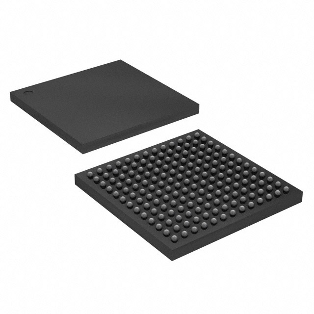
The 10M16SAU169I7G uses a 169-ball UBGA (Ultra Thin Ball Grid Array) package measuring approximately 11 × 11 mm with a 0.8 mm ball pitch. This compact form factor is ideal for space-constrained designs in industrial modules and IoT sensor nodes.
The U169 package provides up to 130 user I/O pins organized across multiple I/O banks, each independently configurable for different voltage standards. Pin assignments should be planned carefully using Intel's Pin Planner tool within Quartus Prime to ensure optimal signal integrity and power distribution.
For PCB layout, maintain a minimum of 4 signal layers with dedicated power and ground planes beneath the BGA footprint. Follow Intel's recommended land pattern and ensure proper thermal relief on the exposed paddle.
5. Typical Application Circuits & Design Tips
The 10M16SAU169I7G excels in applications that require mixed-signal processing, compact size, and instant-on reliability. Common deployment scenarios include:
- Industrial motor control – real-time PWM generation with ADC feedback loops
- IoT edge gateways – protocol bridging (SPI/I2C/UART) with local data preprocessing
- Sensor fusion hubs – multi-channel ADC acquisition with digital filtering in FPGA fabric
- Video preprocessing – low-latency image scaling and color-space conversion
- Test & measurement – custom data acquisition with precise timing control
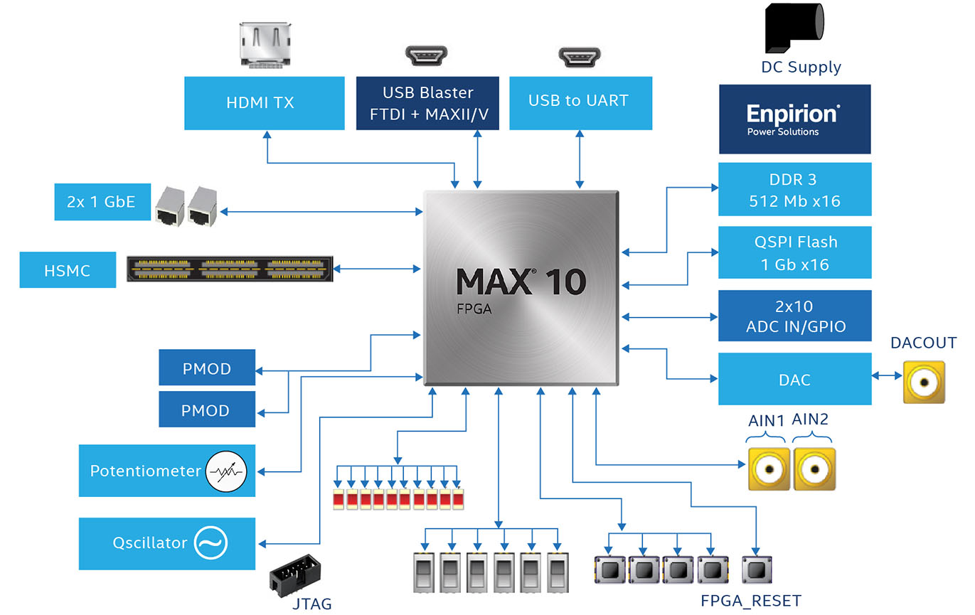
The Terasic DE10-Lite development board provides an affordable platform for prototyping MAX 10 designs, featuring on-board USB-Blaster programming, SDRAM, VGA output, accelerometer, and Arduino-compatible headers. Visit our development board collection for compatible evaluation kits.
Design Tips
- Power sequencing: Bring up VCCINT (1.2 V) before VCCIO banks. The single-supply variant (S) simplifies this with an internal regulator.
- ADC reference: Use a low-noise external 2.5 V reference for the ADC if your application demands > 10-bit effective resolution.
- Decoupling: Place 100 nF capacitors on every VCC pin within 2 mm of the BGA ball. Add bulk 10 µF capacitors near the power entry.
- Configuration: Enable dual-image mode for remote firmware updates with automatic fallback to a known-good image.
Video Tutorial: Getting Started with MAX 10 FPGA
6. FAQ – Frequently Asked Questions
What is the 10M16SAU169I7G?
The 10M16SAU169I7G is a non-volatile FPGA from Intel's (Altera) MAX 10 family. It contains 16,000 logic elements, an integrated dual 12-bit ADC, 549 Kb embedded RAM, 2,304 Kb user flash memory, and 45 DSP multiplier blocks in a compact 169-ball UBGA package. It operates across the industrial temperature range of −40 °C to +100 °C.
Does the 10M16SAU169I7G require an external configuration memory?
No. The MAX 10 family integrates on-die configuration flash memory that stores up to two FPGA configuration images. This enables instant-on operation (boot time under 10 ms) and eliminates the cost and board space of an external serial flash or EEPROM configuration device.
What development tools are needed for the 10M16SAU169I7G?
Intel's Quartus Prime Lite Edition (free download) provides full support for all MAX 10 devices, including synthesis, place-and-route, timing analysis, and JTAG/USB-Blaster programming. ModelSim-Intel FPGA Edition is included for simulation. No paid license is required.
What is the difference between the 10M16SAU169I7G and 10M16SAU169C8G?
Both share the same silicon die and 169-ball UBGA package. The key differences are: the "I7G" variant supports the industrial temperature range (−40 °C to +100 °C) at speed grade 7, while the "C8G" operates over the commercial range (0 °C to +85 °C) at speed grade 8. Choose the I7G for harsh-environment or extended-temperature applications.
How many analog input channels does the 10M16SAU169I7G ADC support?
The integrated dual 12-bit ADC supports up to 18 external analog input channels via an analog multiplexer, plus an internal temperature-sensing diode. Each ADC block can sample at up to 1 MSPS. The ADC requires a 2.5 V analog supply and reference voltage for optimal performance.
Can the 10M16SAU169I7G interface with DDR3 memory?
Yes. The MAX 10 family supports DDR2, DDR3, LPDDR2, and SRAM external memory interfaces through its hard memory controller IP. The U169 package provides sufficient I/O pins for a 16-bit DDR3 interface, though pin count may limit simultaneous use of other high-speed interfaces. Use Intel's External Memory Interface Toolkit in Quartus Prime for automated calibration and timing closure.


