
10M16SAU169I7G Datasheet, Pinout & Application Guide | Altera MAX 10 FPGA
The 10M16SAU169I7G is a non-volatile, single-chip FPGA from Altera's (now Intel) MAX 10 family, fabricated on TSMC's 55 nm flash process. It integrates 16,000 logic elements, 549 Kb of M9K embedded SRAM, 2,304 Kb of user flash memory, 45 hardware 18×18-bit DSP multipliers, 4 PLLs, and a dual 12-bit 1 MSPS SAR ADC — all within a compact 169-ball UBGA package. Operating from a single 3.3 V supply with instant-on boot (under 10 ms), the 10M16SAU169I7G eliminates external configuration memory, reducing BOM cost and board area for industrial control, IoT edge computing, motor drives, and mixed-signal applications.
Overview and Part Number Decoding
The 10M16SAU169I7G belongs to the Altera MAX 10 product line — the industry's first single-chip, non-volatile FPGA family. Unlike SRAM-based FPGAs such as Xilinx Spartan-7 or Intel Cyclone V that require external SPI flash for configuration bitstream storage, MAX 10 devices store up to two complete configuration images in on-die flash memory. This architecture enables instant-on operation within milliseconds of power-up and supports fail-safe remote field updates via the Remote System Upgrade (RSU) IP core — without any external EPCQ or SPI NOR flash on the BOM.
A key differentiator of the “SA” variant is the integrated dual 12-bit, 1 MSPS SAR ADC with up to 18 external analog input channels and an internal temperature sensor. This on-chip ADC eliminates the need for an external ADC IC, saving board space, reducing BOM cost, and simplifying routing in mixed-signal designs such as sensor acquisition, power monitoring, and industrial control.
The part number encodes the following attributes:
- 10M16 — MAX 10 family, 16,000 logic elements
- SA — Single-supply, Analog variant (internal 1.2 V regulator + integrated dual 12-bit ADC)
- U169 — 169-ball Ultra-thin Fine-pitch Ball Grid Array (UBGA), 11 mm × 11 mm
- I7 — Industrial temperature range (−40 °C to +100 °C), speed grade 7
- G — Green / RoHS / Pb-free compliant
The “SA” designation distinguishes this variant from the “SC” (single-supply, compact) variants that omit the analog-to-digital converter. In the SC variant, the analog input pins become general-purpose digital I/O or LVDS channels instead. The industrial-grade “I” temperature rating makes this part ideal for harsh environments including factory automation, outdoor telecom cabinets, and automotive auxiliary systems. The device is fully supported by Intel Quartus Prime Lite Edition, which is free to download and requires no license file. For current stock and pricing, check 10M16SAU169I7G availability on WWDParts.
Specifications and Parameter Table
| Parameter | Value |
|---|---|
| Manufacturer | Altera (Intel) |
| Part Number | 10M16SAU169I7G |
| Family | MAX 10 (10M) |
| Process Technology | 55 nm Flash (TSMC) |
| Logic Elements (LEs) | 16,000 |
| Embedded SRAM (M9K) | 549 Kb (61 M9K blocks) |
| User Flash Memory (UFM) | 2,304 Kb |
| DSP Multipliers (18×18) | 45 |
| PLLs | 4 |
| ADC | Dual 12-bit SAR, 1 MSPS, up to 18 analog inputs |
| Maximum User I/O Pins | 130 |
| LVDS Differential Pairs | Up to 22 |
| External Memory Interface | DDR2, DDR3, LPDDR2, SRAM |
| Configuration Memory | On-die flash, dual-image support |
| Core Voltage | 1.2 V (internal regulator from 3.3 V single supply) |
| I/O Voltage | 1.0 V to 3.3 V (multi-standard per bank) |
| I/O Standards | 3.3 V / 2.5 V / 1.8 V / 1.5 V LVCMOS/LVTTL, SSTL, HSUL, LVDS, differential SSTL |
| Package | 169-ball UBGA (11 mm × 11 mm, 0.8 mm pitch) |
| Temperature Range | −40 °C to +100 °C (Industrial) |
| Speed Grade | 7 (slowest / lowest power) |
| Operating Supply | Single 3.3 V |
| Bitstream Security | AES-256 encryption + JTAG secure mode |
| RoHS / Lead-Free | Yes (Pb-free, Green compliant) |
For equivalent parts, consider the 10M16SAU169C8G (commercial temperature, speed grade 8) or the 10M16SCU169 series (single-supply without ADC) for designs that do not require the integrated analog converter or industrial temperature range.
Architecture and Block Diagram
The MAX 10 architecture is organized around a sea of adaptive logic modules (ALMs), each containing a four-input look-up table (LUT) and a dedicated register. These ALMs are grouped into logic array blocks (LABs) of 16 elements each, interconnected by a hierarchical routing fabric with row, column, and direct-link interconnects that balance speed and routability.
Distributed across the logic fabric are 61 M9K embedded memory blocks (each 9,216 bits) that can be configured as single-port RAM, dual-port RAM, ROM, or shift registers. The 45 embedded multipliers support 9×9, 18×18, or cascaded 36×36-bit operations, making the 10M16 well-suited for digital filtering, sensor signal processing, and motor control algorithms.
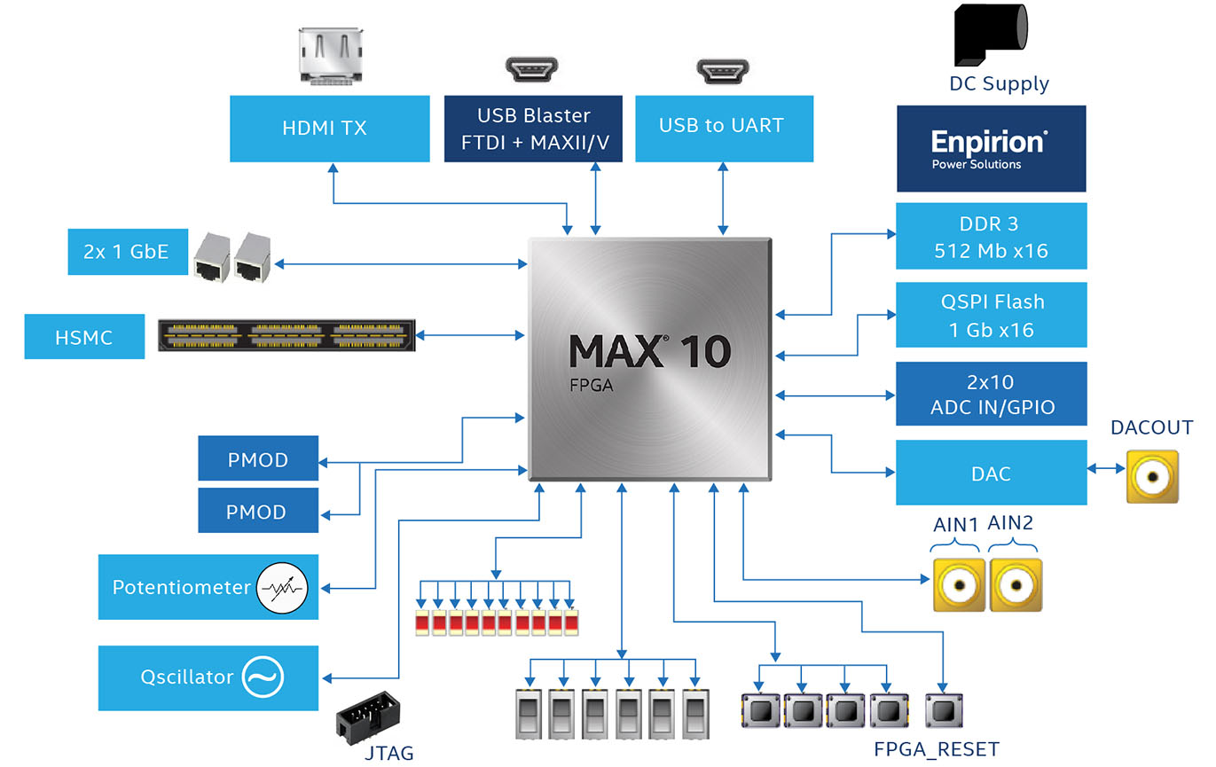
The four general-purpose PLLs provide clock synthesis, multiplication, division, and phase shifting with output frequencies up to 500 MHz. The dual 12-bit ADC blocks are located at dedicated analog input pins and share a common reference voltage. Each ADC channel can be triggered by software, hardware, or a periodic timer, enabling autonomous analog monitoring without consuming logic resources.
The on-die configuration flash memory (CFM) stores up to two full configuration images, enabling a factory image and an application image. The Remote System Upgrade (RSU) controller manages image selection, watchdog timeout, and automatic revert to the factory image if a field update fails — a critical feature for unmanned or hard-to-access installations.
Pinout, Package, and PCB Layout
The 10M16SAU169I7G is housed in a 169-ball UBGA package measuring 11 mm × 11 mm with a 0.8 mm ball pitch. The ultra-thin profile (approximately 1.0 mm height) makes it ideal for space-constrained designs such as SSD controllers, industrial sensor modules, and portable instrumentation.

The 130 user I/O pins are organized into multiple I/O banks, each independently configurable for different voltage standards from 1.0 V to 3.3 V. This multi-standard capability allows direct interfacing with 3.3 V legacy peripherals, 1.8 V DDR3 memory, and 2.5 V LVDS SerDes in a single design without level shifters.
PCB layout guidelines:
- Use a minimum 4-layer stackup: signal–ground–power–signal. Route critical clock and LVDS pairs on inner layers adjacent to a solid ground plane for controlled impedance.
- Place 100 nF ceramic decoupling capacitors within 3 mm of every VCC ball (1.2 V core, 2.5 V PLL, and I/O bank supplies). Add one 10 μF bulk capacitor per supply rail near the package.
- Use 0.3 mm vias with 0.15 mm drill for BGA escape routing. A dog-bone pattern with vias placed 0.5 mm from pad center provides reliable escape for the 0.8 mm pitch grid.
- Route the analog supply (VCCA) through a dedicated ferrite bead and separate analog ground pour to minimize digital noise coupling into the ADC. Keep analog input traces short, guarded, and away from switching I/O.
Application Circuits and Design Guidelines
The 10M16SAU169I7G is widely deployed in industrial automation, IoT edge gateways, motor control, sensor hub applications, and video surveillance pre-processing. Its combination of instant-on operation, integrated ADC, and moderate logic density makes it a natural fit for designs that need real-time analog monitoring alongside digital processing.
Typical application areas:
- Industrial Motor Control: Implement space-vector PWM generation, encoder interface (ABZ / SinCos), and current loop feedback using the integrated ADC — all in a single chip replacing a separate MCU + ADC + CPLD combination.
- IoT Sensor Hub: Aggregate data from multiple analog sensors (temperature, pressure, vibration) via the dual ADC, apply Kalman filtering or FFT in the DSP blocks, and transmit processed data over SPI/I2C/UART to a wireless module.
- Video Pre-Processing: Accept parallel camera data (8/10/12-bit), perform Bayer demosaicing, color correction, and frame buffering in M9K RAM before forwarding to a host processor or display interface.
- Power Supply Sequencing: Use the instant-on capability and internal flash to implement deterministic power rail sequencing and monitoring for complex multi-rail systems, replacing dedicated power management ICs.
Power supply design: The single-supply “SA” variant requires only a 3.3 V ±5% rail; the internal voltage regulator generates the 1.2 V core supply. Total quiescent power is typically 150–250 mW depending on I/O loading and clock frequency. For battery-powered designs, use the standby configuration image with unused I/O tristated and PLLs powered down to minimize static power.
Video Tutorial
Frequently Asked Questions (FAQ)
The “I7” suffix indicates industrial temperature (−40 °C to +100 °C) with speed grade 7, while “C8” denotes commercial temperature (0 °C to +85 °C) with speed grade 8. The I7 variant is tested and guaranteed to operate over a wider temperature range, making it suitable for outdoor, automotive auxiliary, and factory-floor environments. Speed grade 7 is the slowest (lowest power) grade; speed grade 8 offers slightly faster timing at the cost of marginally higher power consumption.
No. The MAX 10 family stores configuration data in on-die flash memory, supporting dual-image storage for factory and application bitstreams. This eliminates the need for external EPCQ or SPI NOR flash, reducing BOM cost and enabling instant-on operation in under 10 ms from power-up.
The dual 12-bit ADC is accessed through the Altera Modular ADC IP core in Quartus Prime. You instantiate the IP, select the desired analog channels (up to 18 external inputs plus the internal temperature sensor), configure the sampling rate (up to 1 MSPS per ADC block), and connect the digital output bus to your logic. The analog inputs accept 0–2.5 V signals referenced to VREFA. For signals outside this range, use a resistive divider or op-amp buffer at the input pins.
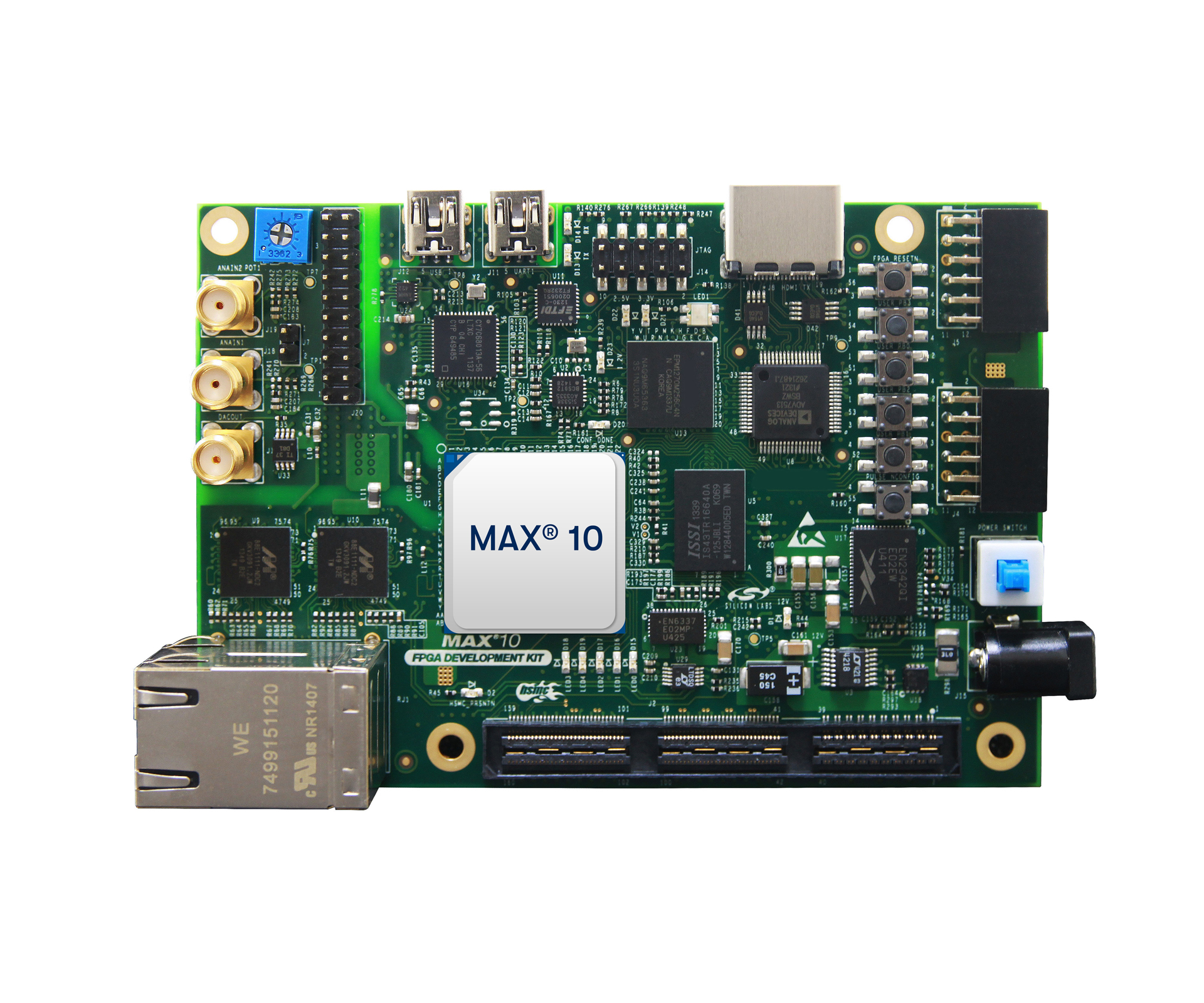
The device is fully supported by Intel Quartus Prime Lite Edition (free, no license required) for synthesis, place-and-route, timing analysis, and JTAG programming. Popular development boards include the MAX 10 FPGA Development Kit (Terasic/Altera) and the Arrow DECA board. Programming is done via an on-board USB-Blaster II or an external USB-Blaster cable connected to the JTAG header.
Yes. The MAX 10 10M16 supports DDR3 SDRAM interfaces at up to 300 MHz (DDR3-600). The external memory interface IP in Quartus Prime generates the required PHY, controller, and calibration logic. However, the 169-UBGA package provides 130 user I/O pins, which limits the addressable DDR3 bus width. For wider memory interfaces, consider the larger U324 or F484 package variants of the 10M16.
Typical quiescent (static) power is approximately 150–250 mW from the single 3.3 V supply, depending on I/O loading and whether the ADC is active. Dynamic power scales with clock frequency, logic utilization, and toggle rate. Use the Intel Early Power Estimator (EPE) spreadsheet or the PowerPlay Power Analysis tool in Quartus Prime for accurate estimates tailored to your specific design. For lowest power, use speed grade 7 and tristate unused I/O pins.
Related components: Explore more Altera FPGA parts on WWDParts — browse MAX 10 FPGA inventory, 10M08SAE144C8G, or EP4CE15F23C8N Cyclone IV.


