
10M16SAU169I7G Datasheet, Specifications & Application Guide – Altera MAX 10 FPGA
Overview of the 10M16SAU169I7G
The 10M16SAU169I7G is a non-volatile FPGA from the Altera (Intel) MAX 10 family, built on TSMC's 55 nm embedded NOR flash process. It delivers 16,000 logic elements in a compact 169-ball UBGA package (11 mm × 11 mm), making it an ideal single-chip solution for industrial control, IoT edge processing, sensor aggregation, and communication control planes. The "I7G" suffix indicates the industrial temperature grade (−40 °C to +100 °C) with speed grade 7, providing reliable operation in harsh environments.
MAX 10 devices uniquely integrate dual configuration flash, an analog-to-digital converter (ADC), and user flash memory on a single die — eliminating external configuration EEPROMs and simplifying BOM costs. The instant-on capability allows the FPGA to be operational within milliseconds of power-up, which is critical for system management and safety applications.
Key Specifications & Parameters
| Parameter | Value |
|---|---|
| Part Number | 10M16SAU169I7G |
| Family | Altera MAX 10 (Intel) |
| Logic Elements (LEs) | 16,000 |
| Logic Array Blocks (LABs) | 1,000 |
| Embedded Memory (M9K Blocks) | 549 Kb (61 blocks) |
| Embedded 18×18 Multipliers | 45 |
| PLLs | 4 |
| Max User I/O Pins | 130 |
| LVDS Pairs | Up to 22 |
| User Flash Memory (UFM) | 2,368 Kb |
| ADC | 1× 12-bit, up to 1 MSPS |
| External Memory Interface | DDR3, DDR2, LPDDR2, SRAM |
| Core Voltage | 1.2 V (1.15–1.25 V) |
| I/O Voltage | 1.0 V to 3.3 V |
| Speed Grade | 7 |
| Temperature Range | −40 °C to +100 °C (Industrial) |
| Package | UBGA-169 (11 mm × 11 mm) |
| Process Technology | 55 nm (NOR Flash) |
| Configuration | Dual internal flash (instant-on) |
| RoHS | Compliant |
Block Diagram & Architecture
The MAX 10 architecture arranges logic, memory, DSP, and I/O resources around a central interconnect fabric. Key functional blocks include the Logic Array Blocks (LABs), M9K embedded memory, 18×18 embedded multipliers for DSP workloads, four PLLs for clock management, a 12-bit SAR ADC, and the User Flash Memory block for on-chip data storage.

The dual-image internal flash configuration allows remote firmware updates with a safe fallback image, while the integrated ADC eliminates the need for external analog front-end ICs in mixed-signal applications.
Pinout & Package Information
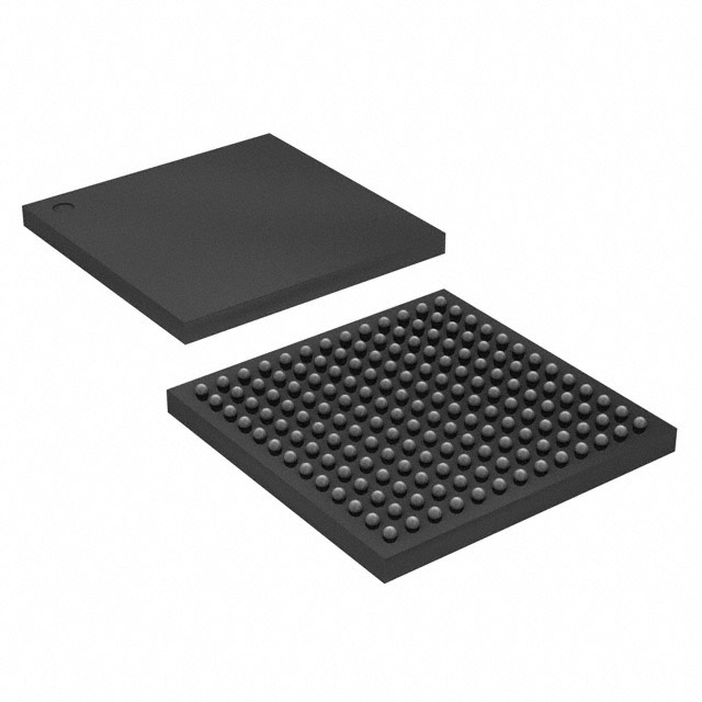
The 10M16SAU169I7G is housed in a 169-ball UBGA package measuring 11 mm × 11 mm × 1 mm, with a 0.8 mm ball pitch. It provides 130 user I/O pins organized across multiple I/O banks supporting LVTTL, LVCMOS (1.0 V to 3.3 V), SSTL, HSTL, and LVDS standards. The compact footprint makes it suitable for space-constrained designs in industrial and consumer electronics.
The UBGA-169 package supports both single-supply and multi-voltage I/O bank configurations, giving designers flexibility in voltage domain partitioning across the device.
Application Circuit & Design Examples
The 10M16SAU169I7G is widely used in industrial automation, motor control, building management systems, communications protocol bridging, and IoT sensor hubs. Its integrated ADC and instant-on flash configuration make it particularly suited for system management controllers and smart sensor nodes.

The MAX 10 FPGA Development Kit provides a reference design platform with dual Gigabit Ethernet, HDMI, USB-UART, DDR3 memory, and Arduino-compatible headers. Designers can leverage Quartus Prime Lite (free) with the Platform Designer (Qsys) tool to build Nios II soft processor systems, ADC data-logging pipelines, and multi-protocol communication bridges.
Video Tutorial: Getting Started with MAX 10 FPGA
Frequently Asked Questions
What is the 10M16SAU169I7G?
The 10M16SAU169I7G is a non-volatile FPGA from the Altera (Intel) MAX 10 family. It features 16,000 logic elements, 549 Kb of embedded memory, a 12-bit ADC, and 2,368 Kb of user flash memory in a 169-ball UBGA package rated for industrial temperatures (−40 °C to +100 °C).
What is the difference between 10M16SAU169I7G and 10M16SAU169C8G?
Both share the same die and package (16K LE, UBGA-169). The key differences are temperature grade and speed: the I7G variant supports industrial temperatures (−40 °C to +100 °C) at speed grade 7, while the C8G supports commercial temperatures (0 °C to +85 °C) at speed grade 8 (slower). Choose I7G for harsh-environment deployments.
Does the 10M16SAU169I7G have a built-in ADC?
Yes. The MAX 10 10M16SAU169I7G integrates a single 12-bit successive-approximation-register (SAR) ADC that supports up to 1 MSPS sampling rate. It can be accessed as an IP block within Quartus Prime and connected to external analog signals through dedicated ADC input pins.
What design software is needed for the 10M16SAU169I7G?
Intel Quartus Prime Lite Edition (free download) fully supports all MAX 10 devices, including the 10M16SAU169I7G. It includes synthesis, place-and-route, timing analysis, the Platform Designer (Qsys) system integration tool, and the Nios II soft processor toolchain.
What external memory does the 10M16SAU169I7G support?
The 10M16SAU169I7G supports DDR3, DDR2, LPDDR2, and SRAM external memory interfaces through its dedicated hard memory controller IP. This enables high-bandwidth data buffering and frame storage for video, communications, and DSP applications.
Where can I buy the 10M16SAU169I7G?
The 10M16SAU169I7G is available from authorized distributors including wwdparts.com, DigiKey, Mouser, Arrow, and Octopart. Check wwdparts.com for competitive pricing, stock availability, and fast shipping on this and other MAX 10 FPGA devices.


