
1. Overview of the 10M16SAU169I7G MAX 10 FPGA
The 10M16SAU169I7G is a non-volatile FPGA from Intel (formerly Altera) belonging to the MAX 10 family. Built on 55nm flash process technology, this device integrates 16,000 logic elements, an analog-to-digital converter (ADC), and internal configuration flash memory into a compact 169-ball UBGA package. It is designed for cost-sensitive, single-chip applications in industrial automation, motor control, communications, and consumer electronics.
Unlike SRAM-based FPGAs that require an external configuration device, the MAX 10 stores its configuration in on-chip flash, enabling instant-on operation within milliseconds of power-up. The 10M16SAU169I7G supports dual configuration images, allowing seamless remote field upgrades with a safe fallback image.
Figure 1: MAX 10 FPGA functional block diagram showing the internal architecture, including logic array blocks, embedded memory, PLLs, ADC, and flash configuration memory.
2. Key Specifications and Parameters
The following table summarizes the critical electrical and functional parameters of the 10M16SAU169I7G. These values are essential for schematic design, power budgeting, and system integration. For the complete datasheet, visit the wwdparts IC chip guide.
| Parameter | Value |
|---|---|
| Part Number | 10M16SAU169I7G |
| Manufacturer | Intel (Altera) |
| Family | MAX 10 (10M16) |
| Process Technology | 55 nm Flash |
| Logic Elements (LEs) | 16,000 |
| Logic Array Blocks (LABs) | 1,000 |
| Embedded Memory (M9K) | 549 Kb (61 M9K blocks) |
| 18x18 Embedded Multipliers | 45 |
| Phase-Locked Loops (PLLs) | 4 |
| Global Clock Networks | 20 |
| ADC | 1 x 12-bit, up to 1 MSPS |
| User I/O (U169 package) | 130 |
| Max LVDS Pairs | 22 |
| Internal Flash (UFM) | 128 Kb User Flash Memory |
| Configuration Flash | Dual-image support |
| Core Voltage (VCCINT) | 1.2 V |
| I/O Voltage | 1.0 V - 3.3 V (multi-standard) |
| Speed Grade | 7 (Industrial) |
| Operating Temperature | -40 C to +100 C |
| Package | UBGA-169 (11 mm x 11 mm) |
| DDR Memory Interface | DDR2, DDR3, LPDDR2 |
| I/O Standards | LVTTL, LVCMOS, SSTL, HSTL, HSUL, LVDS |
| Configuration | Internal (instant-on), JTAG |
| RoHS Compliant | Yes (Lead-free) |
3. Pinout and Package Information
The 10M16SAU169I7G is housed in a 169-ball UBGA (Ultra-thin Ball Grid Array) package measuring 11 mm x 11 mm with a 0.8 mm ball pitch. This compact form factor makes it ideal for space-constrained designs. The device provides 130 user I/O pins supporting a wide range of I/O standards from 1.0 V LVCMOS to 3.3 V LVTTL, along with differential LVDS pairs for high-speed serial interfaces.
Key pin groups include dedicated clock inputs, JTAG programming pins (TDI, TDO, TMS, TCK), power supply pins (VCCINT, VCCIO, GND), and analog input pins for the on-chip ADC. Designers should refer to the official pin-out file available through the wwdparts FPGA programming guide for complete ball-map assignments.

Figure 2: 10M16SAU169I7G in the UBGA-169 package - a compact 11x11 mm BGA form factor with 130 user I/O pins.
4. Typical Applications and Circuit Design
The MAX 10 FPGA family is designed for single-chip, low-power embedded applications. The 10M16SAU169I7G is commonly used in:
- Industrial Automation: Motor control, sensor fusion, and real-time I/O processing using the integrated ADC and embedded multipliers.
- Communications: Protocol bridging, data aggregation, and custom interface adapters leveraging the flexible I/O standards and DDR3 memory interfaces.
- Consumer Electronics: Display controllers, LED drivers, and audio processing benefiting from the compact UBGA-169 footprint and instant-on capability.
- Automotive & Aerospace (Industrial Grade): The -40 C to +100 C temperature range and flash-based reliability make it suitable for harsh-environment designs.
A typical application circuit requires minimal external components: decoupling capacitors for VCCINT (1.2 V) and VCCIO banks, a 3.3 V regulator, JTAG header for programming, and optional DDR3 SDRAM for data-intensive applications. Browse more application notes at the wwdparts development board guide.
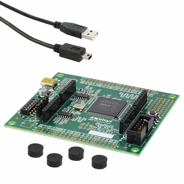
Figure 3: MAX 10 FPGA Evaluation Kit - a reference development board demonstrating typical application circuitry including power regulation, DDR memory, and expansion connectors.
5. Development Tools and Getting Started
Getting started with the 10M16SAU169I7G is straightforward thanks to Intel's free Quartus Prime Lite Edition, which provides full support for the MAX 10 family including synthesis, place-and-route, timing analysis, and the embedded logic analyzer (SignalTap). Key development resources include:
- Quartus Prime Lite Edition: Free FPGA design software with VHDL/Verilog support, IP catalog, and Pin Planner for the U169 package.
- Nios II Processor: A soft-core 32-bit RISC processor that can be instantiated inside the 10M16 for embedded software applications.
- Platform Designer (Qsys): System integration tool for connecting IP blocks, memory controllers, and custom peripherals.
- MAX 10 Evaluation Kits: Available from Arrow, Terasic, and others, providing ready-to-use hardware with USB-Blaster programming.
The following video provides an excellent introduction to the Intel FPGA development workflow with Quartus Prime and the MAX 10 platform:
6. Frequently Asked Questions (FAQ)
Q1: What is the difference between 10M16SAU169I7G and 10M16SAU169C8G?
The "I7G" suffix denotes the industrial temperature range (-40 C to +100 C) with speed grade 7, while "C8G" indicates the commercial temperature range (0 C to +85 C) with speed grade 8. The industrial variant is rated for harsher operating environments but may have a slightly lower maximum clock frequency due to the wider temperature derating.
Q2: Does the 10M16SAU169I7G require an external configuration memory?
No. The MAX 10 FPGA uses internal flash memory to store its configuration, eliminating the need for an external EEPROM or flash device. This enables instant-on operation (typically under 10 ms) and reduces BOM cost and board area. The device supports dual configuration images for safe remote updates.
Q3: How many logic elements does the 10M16SAU169I7G have?
The 10M16SAU169I7G contains 16,000 logic elements (LEs) organized into 1,000 logic array blocks (LABs). It also includes 549 Kb of M9K embedded memory, 45 embedded 18x18 multipliers for DSP functions, and 4 PLLs for clock management.
Q4: Can I use the on-chip ADC in the 10M16SAU169I7G?
Yes. The device includes a 12-bit ADC capable of up to 1 MSPS (mega-samples per second). It supports up to 9 analog input channels (depending on the package and I/O bank configuration) and a built-in temperature sensor. The ADC is configured and controlled through the Quartus Prime Modular ADC IP core.
Q5: What programming interface does the 10M16SAU169I7G use?
The device is programmed via JTAG (IEEE 1149.1) using an Intel USB-Blaster or USB-Blaster II cable. The JTAG interface is also used for in-system debugging with SignalTap logic analyzer. Configuration can also be loaded from internal flash at power-up without any external programmer.
Q6: Is the 10M16SAU169I7G suitable for low-power battery-operated designs?
The MAX 10 family is designed for low-power applications. The 1.2 V core voltage and 55nm flash process contribute to low static power. The device supports multiple power-saving I/O standards and programmable drive strengths. However, for ultra-low-power requirements, designers should carefully analyze the power consumption using the Intel Early Power Estimator (EPE) tool for their specific design utilization.


