
10M16SAU169I7G Datasheet, Specifications & Application Guide | Intel Altera MAX 10 FPGA
The 10M16SAU169I7G is an industrial-grade FPGA from Intel (formerly Altera) belonging to the MAX 10 family. Built on 55nm flash process technology, this non-volatile FPGA integrates 16,000 logic elements, embedded memory, dual ADCs, and user flash memory in a compact UBGA-169 package. Designed for cost-sensitive and space-constrained industrial applications, the 10M16SAU169I7G operates across the full industrial temperature range of -40°C to +100°C, making it ideal for factory automation, motor control, sensor fusion, and IoT edge processing.
Table of Contents
- Key Specifications & Parameters
- Block Diagram & Architecture
- Pinout & Package Information
- Application Circuit & Design Examples
- Video Tutorial & Development Resources
- Frequently Asked Questions
Key Specifications & Parameters
The following table summarizes the critical electrical and functional parameters of the 10M16SAU169I7G MAX 10 FPGA. These specifications are essential for schematic design, component selection, and system integration.
| Parameter | Value |
|---|---|
| Part Number | 10M16SAU169I7G |
| Manufacturer | Intel (Altera) |
| Family | MAX 10 (10M16) |
| Logic Elements (LEs) | 16,000 |
| Logic Array Blocks (LABs) | 1,000 |
| Embedded Memory | 549 Kb (562,176 bits) |
| User Flash Memory | 2,304 Kb |
| 18×18 Multipliers | 45 |
| PLLs | 4 |
| Max User I/O Pins | 130 |
| Max LVDS Pairs | 22 |
| ADC | Dual 12-bit, 1 MSPS |
| Package | UBGA-169 (11mm × 11mm) |
| Core Voltage | 1.2V |
| I/O Voltage | 3.3V / 2.5V / 1.8V / 1.5V |
| Operating Temperature | -40°C to +100°C (Industrial) |
| Speed Grade | 7 |
| Process Technology | 55nm Flash |
| Configuration | Internal flash (instant-on) |
| Supported Memory Interfaces | DDR3, DDR2, LPDDR2, SRAM |
| I/O Standards | LVTTL, LVCMOS, SSTL, HSTL, LVDS, TMDS, PCI |
| RoHS Compliant | Yes (lead-free, "G" suffix) |
Block Diagram & Architecture
The MAX 10 FPGA architecture provides a unique combination of non-volatile flash-based configuration, programmable logic, embedded memory blocks (M9K), DSP blocks with 18×18 multipliers, and an integrated dual analog-to-digital converter (ADC). The instant-on capability eliminates the need for external configuration devices, reducing BOM cost and board area. The 10M16SAU169I7G features four PLLs for flexible clock management and supports both single-supply and dual-supply I/O modes.

Figure 1: MAX 10 FPGA Development Kit block diagram illustrating the internal functional blocks and interconnect structure of the MAX 10 platform.
Pinout & Package Information
The 10M16SAU169I7G comes in a 169-ball UBGA (Ultra Fine-pitch Ball Grid Array) package measuring 11mm × 11mm with a 0.8mm ball pitch. This compact form factor makes it well suited for space-constrained designs in industrial, IoT, and portable applications. The device provides up to 130 user I/O pins with support for multiple I/O voltage standards including 3.3V LVTTL, 2.5V LVCMOS, 1.8V, and differential LVDS signaling. Pin migration is available within the MAX 10 U169 package family, allowing designers to scale between 10M02, 10M04, 10M08, and 10M16 devices without PCB redesign.
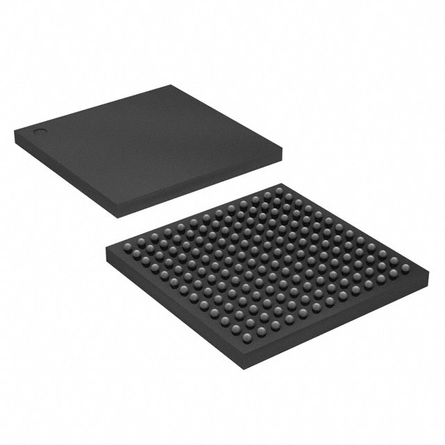
Figure 2: 10M16SAU169I7G MAX 10 FPGA in UBGA-169 package — the compact 11mm × 11mm BGA form factor with 130 user I/O pins.
Application Circuit & Design Examples
The 10M16SAU169I7G is commonly used in designs requiring low-power programmable logic with integrated analog capabilities. Typical application circuits include:
- Sensor Hub / IoT Gateway: Leverage the built-in dual ADC to directly digitize analog sensor inputs, while the FPGA logic handles protocol bridging (SPI, I²C, UART) and data preprocessing before passing to a host MCU or wireless module.
- Motor Control: Implement high-performance PWM generation, encoder feedback processing, and PID control loops. The instant-on feature ensures the motor controller is operational immediately after power-up.
- Industrial Protocol Converter: Use the 16K LEs to implement real-time protocol conversion between Modbus, EtherCAT, PROFINET, or other industrial fieldbus standards.
- Video/Image Pre-processing: The 549 Kb embedded memory and 45 DSP multiplier blocks support pixel-level filtering, color space conversion, and basic image recognition at the edge.
Intel provides reference designs through the MAX 10 FPGA Development Kit, which includes Gigabit Ethernet, HDMI, USB, and HSMC expansion interfaces for rapid prototyping.

Figure 3: Intel MAX 10 FPGA Development Kit — an evaluation platform for prototyping designs using MAX 10 devices including the 10M16 series.
Video Tutorial & Development Resources
Getting started with the 10M16SAU169I7G and the MAX 10 FPGA family is straightforward using Intel's free Quartus Prime Lite Edition software. The toolchain supports design entry via Verilog, VHDL, or schematic capture, along with built-in simulation, timing analysis, and pin planning. The following video provides an introduction to FPGA development with the MAX 10 platform:
Video: Introduction to Intel MAX 10 FPGA development and Quartus Prime design flow.
Development Resources
- Quartus Prime Lite: Free FPGA design software with full MAX 10 support
- Platform Designer (Qsys): System integration tool for Nios II soft processor and peripheral IP
- MAX 10 FPGA Device Handbook: Complete architecture reference and design guidelines
- Intel FPGA IP Library: Pre-verified IP cores for DDR3, PCI Express, Ethernet, and more
Frequently Asked Questions
What is the difference between 10M16SAU169I7G and 10M16SAU169C8G?
The main differences are temperature range and speed grade. The 10M16SAU169I7G is the industrial variant operating from -40°C to +100°C with speed grade 7 (faster), while the 10M16SAU169C8G is the commercial variant operating from 0°C to +85°C with speed grade 8 (slower). Both share the same logic capacity (16,000 LEs) and UBGA-169 package. Choose the I7G version for harsh-environment applications requiring wider temperature tolerance and higher performance.
Does the 10M16SAU169I7G require an external configuration memory?
No. The MAX 10 FPGA family features internal flash-based configuration, which means the device stores its configuration bitstream in on-chip non-volatile memory. This provides instant-on operation — the FPGA is fully configured and functional within milliseconds of power-up, without needing an external EPROM, flash chip, or configuration controller. This reduces BOM cost, board area, and simplifies the supply chain.
What software do I need to program the 10M16SAU169I7G?
You need Intel Quartus Prime Lite Edition, which is available as a free download from Intel's website. It provides full support for all MAX 10 devices including design entry (Verilog/VHDL/schematic), synthesis, place-and-route, timing analysis, and JTAG programming. For system-level design with the Nios II soft processor, use the integrated Platform Designer (formerly Qsys) tool.
Can the 10M16SAU169I7G interface with DDR3 memory?
Yes. The MAX 10 10M16 device supports external memory interfaces including DDR3, DDR2, LPDDR2, and SRAM. The device includes dedicated I/O circuitry and DLL support for high-speed memory interfaces. However, note that the U169 package has limited I/O count (130 pins), so a DDR3 implementation may consume a significant portion of available I/O. For designs requiring wide DDR3 buses, consider the larger F484 or U324 package options.
What is the built-in ADC specification of the 10M16SAU169I7G?
The 10M16SAU169I7G integrates a dual 12-bit SAR ADC with a maximum sampling rate of 1 MSPS (mega samples per second). Each ADC block supports up to 9 analog input channels that can be multiplexed. The ADC operates from a separate analog supply and includes an internal voltage reference, temperature sensor, and programmable sample timing. This eliminates the need for external ADC chips in many sensor acquisition and monitoring applications.
Where can I buy the 10M16SAU169I7G and what is its availability?
The 10M16SAU169I7G is available from authorized distributors including Digi-Key, Mouser Electronics, Arrow, and Newark/element14. You can also source it from wwdparts.com which provides competitive pricing, stock availability, and fast global shipping for industrial and commercial quantities. Always verify the date code and ensure parts come from authorized supply chains to avoid counterfeit risk.
Related Products & Resources
Explore more FPGA and semiconductor components at wwdparts.com:


