
The 10M16SAU169I7G is a non-volatile FPGA from the Altera (Intel) MAX 10 family, built on a 55 nm process node. Featuring 16,000 logic elements, a dual 12-bit ADC, 549 Kb of embedded SRAM, and instant-on configuration from internal flash memory, this industrial-grade device delivers a unique combination of FPGA flexibility and CPLD-like simplicity in a compact 169-ball UBGA package. It is widely used in industrial control, motor drives, sensor hubs, IoT edge computing, and mixed-signal data acquisition systems.
Overview & Part Number Decoding
The 10M16SAU169I7G belongs to the Intel (formerly Altera) MAX 10 FPGA family — the industry's first single-chip, non-volatile FPGA. Unlike traditional FPGAs that require an external configuration flash, MAX 10 devices store their configuration in on-chip flash memory, enabling instant-on operation in under 10 milliseconds. This eliminates an external component, simplifies the PCB layout, and reduces overall BOM cost.
Part number breakdown:
- 10M16 – MAX 10 family, 16,000 logic elements
- S – Single power-supply mode (powered from a single 3.3 V rail)
- A – Analog block enabled (dual 12-bit ADC)
- U169 – 169-ball UBGA package (11 × 11 mm)
- I – Industrial temperature range (−40 °C to +100 °C)
- 7 – Speed grade 7
- G – RoHS-compliant, lead-free packaging
Looking for other MAX 10 FPGA variants? Browse our selection of Intel/Altera FPGA components for competitive pricing and fast shipping.
Key Specifications & Parameters
| Parameter | Value |
|---|---|
| Manufacturer | Altera (Intel) |
| Family | MAX 10 (10M16) |
| Process Technology | 55 nm |
| Logic Elements (LEs) | 16,000 |
| Logic Array Blocks (LABs) | 1,000 |
| Embedded SRAM (M9K) | 549 Kb |
| User Flash Memory (UFM) | 2,304 Kb |
| DSP Blocks (18 × 18 multipliers) | 45 |
| PLLs | 4 |
| ADC | Dual 12-bit, up to 1 MSPS |
| Maximum User I/O | 130 |
| Package | 169-UBGA (11 × 11 mm, 0.8 mm pitch) |
| Core Voltage | 1.2 V |
| I/O Supply Voltage | 2.85 V – 3.465 V (3.3 V typical) |
| Operating Temperature | −40 °C to +100 °C (Industrial) |
| Speed Grade | 7 |
| Max Clock Frequency | 200 MHz (fabric), up to 500 MHz (PLL output) |
| Configuration | Internal flash (instant-on, < 10 ms) |
| I/O Standards Supported | LVCMOS, LVTTL, SSTL, HSTL, LVDS |
| RoHS Compliant | Yes (lead-free) |
Need to source the 10M16SAU169I7G? Check our real-time inventory and pricing at WWDParts.
Architecture & Block Diagram
The MAX 10 architecture integrates a rich set of resources on a single monolithic die. At its core, the Logic Array Block (LAB) consists of 16 logic elements (LEs), each containing a 4-input look-up table (LUT), a programmable register, and carry-chain logic optimized for arithmetic. The 10M16 variant provides 1,000 LABs totaling 16,000 LEs.
Surrounding the logic fabric are 549 Kb of M9K embedded memory blocks (each 9 Kb, dual-port, operating up to 284 MHz), 45 DSP blocks for hardware-accelerated multiply-accumulate operations, and four fabric PLLs supporting clock management up to 500 MHz. The integrated dual 12-bit ADC enables direct analog sensor interfacing without external conversion circuitry.
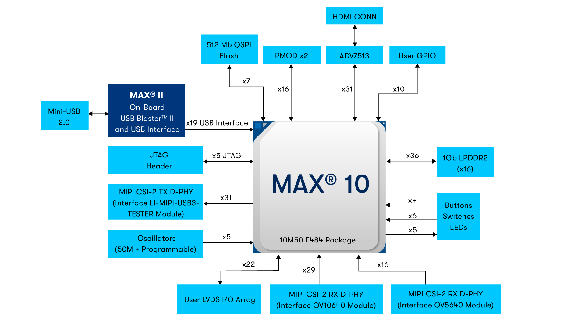
Figure 1: MAX 10 FPGA system architecture block diagram illustrating the integration of logic, memory, DSP, ADC, and I/O resources.
Pinout & Package Information
The 10M16SAU169I7G is housed in a 169-ball UBGA (Ultra-thin Ball Grid Array) package with an 11 × 11 mm body and 0.8 mm ball pitch. This compact form factor is well-suited for space-constrained embedded designs while still providing 130 user-configurable I/O pins organized across multiple I/O banks.
Key pinout highlights:
- 130 user I/O pins supporting LVCMOS (1.2 V – 3.3 V), LVTTL, SSTL, HSTL, and LVDS standards
- Dedicated configuration pins for JTAG (TCK, TMS, TDI, TDO) and optional passive serial (nCONFIG, nSTATUS, CONF_DONE)
- Analog input pins for the on-chip dual 12-bit ADC channels
- Power supply pins for VCCIO (3.3 V), VCCINT (1.2 V), and analog supply (VCCADC)

Figure 2: MAX 10 FPGA in the 169-ball UBGA package — compact 11 × 11 mm BGA form factor used by the 10M16SAU169I7G.
For complete pin assignment tables and I/O bank voltage mappings, refer to the official Intel MAX 10 Pin Information document or download the package files from WWDParts technical blog.
Application Circuits & Design Guide
The 10M16SAU169I7G excels in applications that demand FPGA-level flexibility with CPLD-like simplicity. Its single 3.3 V power-supply mode, instant-on configuration, and integrated ADC make it an ideal fit for:
- Industrial control & motor drives – Real-time PWM generation, encoder interfaces, and closed-loop control with on-chip ADC for current sensing.
- Sensor fusion & IoT edge gateways – Aggregate data from multiple analog and digital sensors, perform local filtering/processing, and forward results via SPI, I²C, or UART.
- Video surveillance pre-processing – Pixel-level image processing, overlay generation, and protocol bridging (MIPI CSI-2, parallel camera interfaces).
- Medical instrumentation – Precision data acquisition using the 12-bit ADC, combined with custom digital filtering implemented in the FPGA logic.
- Building automation – Multi-channel monitoring and control with instant-on for safety-critical subsystems.

Figure 3: MAX 10 FPGA 10M50 Evaluation Kit — a reference design platform demonstrating typical application circuits including ADC interfacing, HDMI output, and memory connectivity.
Design tips:
- Use Quartus Prime Lite Edition (free) for synthesis, place-and-route, and JTAG programming of all MAX 10 devices.
- Enable the "single supply" configuration mode to simplify your power design — only a single 3.3 V rail is needed.
- Take advantage of the User Flash Memory (UFM) for storing calibration data, firmware parameters, or small lookup tables without requiring external EEPROM.
- Leverage the four fabric PLLs for clean clock generation and frequency synthesis up to 500 MHz.
Video Tutorial: Getting Started with Intel MAX 10 FPGA
Watch this tutorial to learn the complete Intel FPGA development workflow using Quartus Prime with a MAX 10 device — from design entry through programming.
Frequently Asked Questions
What is the 10M16SAU169I7G?
The 10M16SAU169I7G is a non-volatile FPGA from the Altera (Intel) MAX 10 family built on 55 nm technology. It features 16,000 logic elements, a dual 12-bit ADC, 549 Kb of embedded SRAM, and 2,304 Kb of user flash memory in a compact 169-ball UBGA package with industrial temperature range (−40 °C to +100 °C).
What is the operating temperature range of the 10M16SAU169I7G?
The 10M16SAU169I7G operates across the industrial temperature range from −40 °C to +100 °C, as indicated by the "I" suffix in the part number. This makes it suitable for demanding industrial, automotive peripheral, and outdoor deployed applications.
Does the 10M16SAU169I7G have an integrated ADC?
Yes. The 10M16SAU169I7G integrates a dual-channel 12-bit successive-approximation ADC capable of up to 1 MSPS per channel. This eliminates the need for an external ADC in many mixed-signal designs, reducing BOM cost and board area.
What package type does the 10M16SAU169I7G use?
It uses a 169-ball UBGA (Ultra-thin Ball Grid Array) package measuring approximately 11 × 11 mm with a 0.8 mm ball pitch. This compact surface-mount package provides 130 user I/O pins and is ideal for space-constrained designs.
What software tools are needed to program the 10M16SAU169I7G?
Intel Quartus Prime Lite Edition (free) supports all MAX 10 devices including the 10M16SAU169I7G. It provides synthesis, place-and-route, timing analysis, and JTAG programming. The design can be entered using Verilog, VHDL, or schematic capture.
What are common applications for the 10M16SAU169I7G?
Common applications include industrial control and motor drives, sensor fusion and IoT edge gateways, video surveillance pre-processing, medical instrumentation, building automation, and automotive peripheral systems. Its integrated ADC and instant-on capability make it especially suited for mixed-signal industrial designs.


