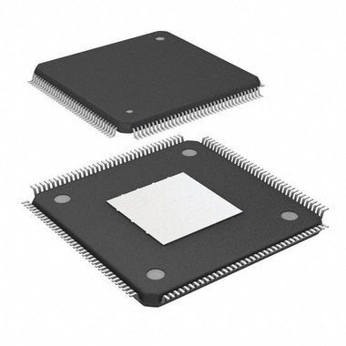
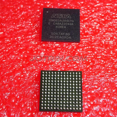
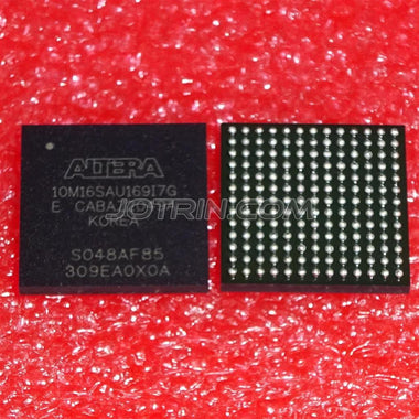
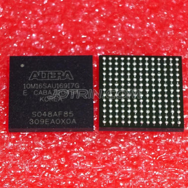
The 10M04SCE144C8G is a non-volatile, single-chip FPGA from Intel's (formerly Altera) MAX 10 family, fabricated on TSMC's 55 nm flash process. It integrates 4,000 logic elements, 189 Kbit of M9K embedded SRAM, 16 hardware 18×18-bit multipliers, dual on-die configuration flash images, 1,376 Kbit of user flash memory, and 2 PLLs — all within a compact 144-pin EQFP package. Operating from a single 3.3 V supply with instant-on boot (under 10 ms), the device eliminates external configuration memory, reducing BOM cost and board area for embedded, industrial, and IoT edge applications.
Overview and Part Number Decoding
The 10M04SCE144C8G belongs to the Intel MAX 10 product line — the industry's first single-chip, non-volatile FPGA family. Unlike SRAM-based FPGAs such as Xilinx Spartan or Intel Cyclone that require external SPI flash for configuration bitstream storage, MAX 10 devices store up to two complete configuration images in on-die flash memory. This architecture enables instant-on operation within milliseconds of power-up and supports fail-safe remote field updates via the Remote System Upgrade (RSU) IP core — without any external EPCQ or SPI NOR flash on the BOM.
The part number encodes the following attributes:
- 10M04 — MAX 10 family, 4,000 logic elements
- SC — Single-supply, Compact variant (internal 1.2 V regulator, no integrated ADC)
- E144 — 144-pin Enhanced Quad Flat Package (EQFP) with exposed thermal pad
- C8 — Commercial temperature range (0 °C to +85 °C), speed grade 8
- G — Green / RoHS / Pb-free compliant
The "SC" designation distinguishes this variant from the "SA" (single-supply, analog) variants that include a 12-bit, 1 MSPS SAR ADC. In the SC variant, the analog input pins are instead available as general-purpose digital I/O or LVDS channels. The device is fully supported by Intel Quartus Prime Lite Edition, which is free to download and requires no license file. For availability and pricing, check 10M04SCE144C8G inventory and pricing on WWDParts.
Specifications and Parameter Table
| Parameter | Value |
|---|---|
| Manufacturer | Intel (Altera) |
| Product Family | MAX 10 |
| Part Number | 10M04SCE144C8G |
| Logic Elements (LEs) | 4,000 |
| Logic Array Blocks (LABs) | 250 (16 LEs per LAB) |
| M9K Embedded Memory Blocks | 21 |
| Total Embedded SRAM | 189 Kbit |
| 18×18 Embedded Multipliers | 16 |
| Phase-Locked Loops (PLLs) | 2 (4 output counters each) |
| User Flash Memory (UFM) | 1,376 Kbit |
| Configuration Flash Memory | Dual-image internal flash (instant-on) |
| User I/O Pins (E144 package) | 101 |
| I/O Banks | 8 |
| Maximum LVDS Differential Pairs | 15 |
| I/O Standards Supported | 3.3 V / 2.5 V / 1.8 V / 1.5 V LVTTL/LVCMOS, LVDS, SSTL, HSTL |
| Maximum Fabric Frequency | 402 MHz |
| M9K Maximum Speed | 284 MHz |
| Core Voltage (VCC) | 1.2 V (internally regulated from 3.3 V) |
| External Supply (VCCA / VCCIO) | 3.3 V single rail (2.85–3.15 V range) |
| Process Technology | 55 nm (TSMC) |
| Package | 144-EQFP (20 × 20 mm body, 0.5 mm pitch, exposed pad) |
| Operating Temperature | 0 °C to +85 °C (Commercial) |
| Speed Grade | 8 |
| Integrated ADC | No (SC Compact variant; use 10M04SAE144C8G for ADC) |
| RoHS Compliant | Yes (Pb-free) |
| Lifecycle Status | Active (2026) |
Architecture and Block Diagram
The MAX 10 FPGA architecture is organized around a fabric of configurable logic, embedded memory, and DSP resources interconnected by a hierarchical routing network with 20 global clock networks. The 10M04SCE144C8G integrates the following core building blocks:
- 4,000 Logic Elements (LEs): Each LE contains a 4-input look-up table (LUT), a programmable register with synchronous load and asynchronous clear, carry chain logic, and register feedback. LEs are grouped into 250 Logic Array Blocks (LABs) of 16 LEs each, with dedicated local interconnect enabling fast intra-LAB routing at minimal skew.
- 21 M9K Memory Blocks (189 Kbit): Each 9,216-bit block (including parity) is configurable as single-port RAM, simple dual-port RAM, true dual-port RAM, ROM, or FIFO buffer. Supports data widths from ×1 to ×36 with byte-enable control, operating at up to 284 MHz. The memory blocks are column-organized for deterministic timing.
- 16 Embedded 18×18-bit Multipliers: Dedicated DSP blocks for arithmetic operations. Each block can operate as one 18×18-bit multiplier or be split into two independent 9×9-bit multipliers — ideal for FIR filters, PID control loops, motor drive algorithms, and fixed-point arithmetic pipelines.
- 2 PLLs: On-chip phase-locked loops provide clock synthesis, multiplication (up to ×512), division, and dynamic phase shifting. Input frequency range spans 5 MHz to 472.5 MHz with up to 4 independent output clocks per PLL. Each PLL includes lock detect and dynamic reconfiguration capabilities.
- Dual Configuration Flash + 1,376 Kbit UFM: Two on-die configuration images enable fail-safe remote field updates via the Remote System Upgrade (RSU) IP core. The User Flash Memory stores calibration constants, serial numbers, encryption keys, or small firmware data non-volatilely — accessible at runtime through the UFM IP core or Avalon-MM interface.

Figure 1: Intel MAX 10 FPGA family architecture — configurable logic fabric, embedded memory columns, PLLs, DSP blocks, user flash, and I/O ring. The 10M04SCE144C8G uses this architecture with 4K LEs and 21 M9K blocks.
Pinout, Package, and PCB Layout
The 10M04SCE144C8G is housed in a 144-pin EQFP (Enhanced Quad Flat Package) with a body size of 20 mm × 20 mm, 0.5 mm lead pitch, and a bottom-side exposed thermal pad. The package provides 101 user I/O pins organized across 8 I/O banks, each with an independent VCCIO supply rail for mixed-voltage interfacing.
Key pinout and layout considerations:
- VCCIO Banks: Each I/O bank supports independent VCCIO supply. For the "SC" single-supply variant, all VCCIO pins are typically tied to 3.3 V. Mixed-voltage designs can set individual banks to 2.5 V, 1.8 V, or 1.5 V for direct interfacing to external ICs.
- JTAG Pins (TCK, TDI, TDO, TMS): Dedicated configuration and boundary-scan pins. Apply 10 kΩ pull-up resistors on TDI and TMS, even when JTAG is unused in production — these pins must not float.
- MSEL[0]: Configuration mode select. Tie to GND for internal configuration mode (standard for MAX 10 instant-on operation).
- Power / Ground: All VCC and GND pins must be connected. Place 100 nF MLCC decoupling capacitors on every power pin, plus a 10 µF bulk capacitor per supply rail near the device.
- Exposed Thermal Pad: The center pad on the package bottom must be soldered to a continuous ground plane for thermal dissipation and electrical grounding. Use a minimum of 9 thermal vias (0.3 mm drill) under the pad connecting to inner ground planes.
- LVDS Pairs: Up to 15 true differential LVDS pairs are available. Route with 100 Ω differential impedance, matched-length, on inner PCB layers.

Figure 2: 10M04SCE144C8G in 144-EQFP package — 20 × 20 mm body, 0.5 mm pitch leads, exposed thermal pad on the underside.
Application Circuits and Design Guidelines
The 10M04SCE144C8G is widely deployed in systems that demand instant-on, non-volatile programmable logic with a minimal component count. Typical application domains include:
- Industrial Automation: Motor drive encoder interfaces, PLC I/O expansion modules, sensor aggregation hubs, and protocol bridging (SPI ↔ UART, I2C ↔ parallel bus). The instant-on capability ensures deterministic control outputs within milliseconds of power-up.
- Communications Equipment: Small-cell baseband glue logic, Ethernet MAC-to-PHY bridging, CPRI/OBSAI framing, and multi-protocol serial conversion. The 16 embedded multipliers handle DSP pre-processing in the datapath.
- Board Management Controllers: Voltage rail power sequencing, system health monitoring (temperature, current), fan speed control, and watchdog supervision. The dual-image flash enables safe firmware updates in the field.
- IoT and Edge Computing: Smart sensor hubs, LED matrix display controllers, HMI panel interfaces, and compact data loggers. The 1,376 Kbit UFM provides non-volatile storage for calibration data and event logs without external EEPROM.
Power Supply Design: The "SC" single-supply variant requires only a single 3.3 V rail (2.85–3.15 V). The internal 1.2 V core regulator draws approximately 50–150 mA depending on logic utilization and clock frequency. Texas Instruments reference design TIDA-00607 demonstrates a complete MAX 10 power solution using the TPS65218 PMIC from a single 5 V or Li-Ion input. For battery-operated designs, the MAX 10 supports a low-power standby mode with all I/O held in a known state.
PCB Layout Best Practices:
- Use a 4-layer minimum stackup (signal–ground–power–signal) with dedicated power and ground planes
- Route clock signals on inner layers with 50 Ω controlled impedance; use 100 Ω differential for LVDS pairs
- Keep PLL input clock trace lengths under 50 mm with length-matched output clock routing
- Provide a 10-pin JTAG header (2×5, 2.54 mm pitch) with trace lengths under 150 mm
- Tie MSEL[0] to GND for internal configuration; device boots in under 10 ms from power-up
To browse other Intel FPGA parts in the MAX 10 family and check current availability, visit the MAX 10 series catalog on WWDParts.

Figure 3: MAX 10 FPGA development board — a typical application platform for the 10M04SCE144C8G showing power supply, JTAG programming, and I/O expansion.
Video: Getting Started with Intel MAX 10 FPGA Development
Video: Getting started with Intel MAX 10 FPGA development — demonstrating Quartus Prime workflow applicable to the 10M04SCE144C8G.
Equivalents, Cross-Reference, and Lifecycle
The 10M04SCE144C8G carries an Active lifecycle status as of 2026 and is broadly stocked by major distributors including Digi-Key, Mouser, Arrow, and LCSC. No Product Discontinuation Notice (PDN) has been issued.
Pin-compatible alternatives within the MAX 10 family:
- 10M04SAE144C8G — The "SA" analog variant in the same 144-EQFP package. Pin-compatible drop-in that adds an integrated 12-bit, 1 MSPS SAR ADC with up to 9 analog channels and an internal temperature sensor. No PCB redesign required.
- 10M08SCE144C8G — Same package, doubled to 8,000 LEs with 378 Kbit embedded RAM and 36 M9K blocks. Pin-compatible logic capacity upgrade for designs that outgrow the 10M04.
- 10M04SCE144I7G — Industrial temperature variant (–40 °C to +100 °C) with speed grade 7. Same pinout and package for harsh-environment and automotive-adjacent deployments.
Cross-vendor alternatives:
- Lattice MachXO3LF-4300 (LCMXO3LF-4300C-5BG256C): Comparable logic density (~4,300 LUTs) with integrated flash configuration in a BGA package. Non-volatile instant-on behavior similar to MAX 10. Requires full re-synthesis in Lattice Diamond; pinout is not compatible.
- Microchip PolarFire MPF100T: Higher-density, low-power flash-based FPGA for applications that outgrow MAX 10 capacity. Offers transceiver lanes and significantly more logic, but at higher cost.
Unit pricing for the 10M04SCE144C8G typically falls in the $8–$15 USD range depending on quantity and distribution channel. To check real-time stock, pricing, or request a quote, upload your BOM to WWDParts for fast processing.
Frequently Asked Questions (FAQ)
Does the 10M04SCE144C8G include an integrated ADC?
No. The "SC" (Single-supply, Compact) variant does not include the analog-to-digital converter. For on-chip ADC functionality, use the pin-compatible 10M04SAE144C8G ("SA" variant), which provides a 12-bit, 1 MSPS SAR ADC with up to 9 external analog channels and an internal temperature sensor. The SA variant is a direct drop-in replacement in the same 144-EQFP package.
What development tools and software are required for the 10M04SCE144C8G?
Intel Quartus Prime Lite Edition (free, no license required) fully supports all MAX 10 devices for design entry, synthesis, place-and-route, and timing analysis. A USB-Blaster or USB-Blaster II JTAG programmer cable is needed for device programming and SignalTap logic analyzer debugging. The Quartus package includes Platform Designer (formerly Qsys) for system integration and ModelSim-Intel FPGA Starter Edition for RTL simulation. Both Verilog and VHDL design entry are supported.
Can the 10M08SCE144C8G replace the 10M04SCE144C8G without PCB changes?
Yes. The 10M08SCE144C8G is fully pin-compatible in the same 144-EQFP package and doubles the logic capacity to 8,000 LEs with 378 Kbit of embedded SRAM (42 M9K blocks). Power consumption increases moderately under full logic utilization, so verify that your 3.3 V supply has adequate current margin (typically 20–30 mA additional). Only re-synthesis and re-programming in Quartus Prime are required — no hardware changes.
How fast does the 10M04SCE144C8G boot after power-on?
MAX 10 devices with internal configuration flash complete initialization and become fully operational in under 10 milliseconds after all supply voltages reach valid levels. This instant-on capability is essential for power sequencing controllers, safety interlocks, and any application where I/O pins must reach a known, deterministic state immediately at startup — before external processors or microcontrollers have finished their own boot sequences.
What is the maximum operating frequency of the 10M04SCE144C8G?
The logic fabric supports clock frequencies up to 402 MHz for register-to-register paths at speed grade 8. M9K embedded memory blocks operate at up to 284 MHz. Actual achievable frequency depends on design complexity, routing congestion, and timing constraints set in Quartus Prime TimeQuest Timing Analyzer. The two on-chip PLLs accept input clocks from 5 MHz to 472.5 MHz and provide clock multiplication up to ×512.
Is the 10M04SCE144C8G suitable for automotive or extreme-temperature environments?
The C8G variant is rated for the commercial temperature range (0 °C to +85 °C) only. For extended temperature requirements, use the 10M04SCE144I7G industrial variant (–40 °C to +100 °C), which is pin-compatible and available in the same 144-EQFP package. For AEC-Q100 automotive-grade qualification, contact Intel/Altera or your authorized distributor to confirm the specific device grade and qualification status for your target application.

Alan Carter
Senior Hardware Engineer & Component Specialist
Alan has over 15 years of expertise in embedded systems design, FPGA architecture, and global semiconductor supply chains. He specializes in component cross-referencing, lifecycle management, and helping OEMs navigate supply shortages.