Chip Manufacturing - How are Microchips made? | Infineon
2026 Executive Summary: A Computer Chip (Integrated Circuit) is the fundamental building block of modern electronics, packing billions of nanometer-scale transistors onto a semiconductor wafer. In 2026, chip technology is defined by 2nm manufacturing nodes, AI-dedicated architectures (NPUs), and heterogeneous "Chiplet" designs that power everything from autonomous vehicles to generative AI models.
| Topics covered in this article: |
| Ⅰ. What is a Chip? (2026 Definition) |
| Ⅱ. Classification: ASIC, SoC, FPGA & AI Accelerators |
| Ⅲ. The Chip Design Process: Step-by-Step |
Ⅰ. What is a Computer Chip? (2026 Definition)
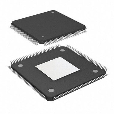
A computer chip, officially known as an Integrated Circuit (IC), is a compact electronic unit comprised of billions of microscopic transistors, resistors, and capacitors fabricated on a thin semiconductor wafer. In 2026, these devices are the "brains" of all digital technology, evolving from simple logic gates to complex Neural Processing Units (NPUs) capable of running Generative AI models.
While early chips contained a few thousand transistors, modern 2026 flagship processors (fabricated on 2nm and 3nm process nodes) routinely pack over 100 billion transistors into an area smaller than a fingernail. Silicon remains the dominant raw material due to two critical properties:
-
Semiconductivity: Silicon can act as both a conductor and an insulator depending on "doping" (the addition of impurities like phosphorus or boron), allowing for precise control of electrical current.
-
Economic Scalability: Silicon is the second most abundant element in the Earth's crust, making it a cost-effective base for mass production, though specialized materials like Gallium Nitride (GaN) and Silicon Carbide (SiC) are now preferred for high-power electric vehicle (EV) applications.
Chips are rarely standalone; they are purpose-built for industries ranging from aerospace to consumer electronics. To function, one or more ICs are mounted onto a Printed Circuit Board (PCB), connecting them to memory, power management modules, and input/output interfaces via microscopic copper pathways.

Ⅱ. Classification: ASIC, SoC, FPGA & AI Accelerators
Chips are classified based on their functionality, programmability, and integration level. In the AI era of 2026, the distinctions have evolved, with Heterogeneous Computing (combining different types of processors) becoming the standard.

1. Application Specific Integrated Circuit (ASIC)
An ASIC is a custom chip designed for a singular, permanent purpose—such as mining cryptocurrency, processing radar signals, or accelerating specific AI training workloads. Once manufactured, its logic cannot be changed.
-
Efficiency: Highest possible performance-per-watt for its specific task.
-
Cost: Extremely high upfront design cost (millions of dollars), but very low unit cost in mass production.
-
Use Case: Bitcoin miners, AI Training Clusters (e.g., Google TPU), Automotive Radar.
2. System on Chip (SoC)
The SoC is the dominant architecture for mobile devices and laptops in 2026. It integrates all critical system components—CPU, GPU, NPU (Neural Processing Unit), memory controller, and radios (5G/6G)—onto a single piece of silicon.
-
Integration: Combines digital, analog, mixed-signal, and radio-frequency functions.
-
Modern Context: 2026 SoCs focus on "Heterogeneous Integration," ensuring the AI workload goes to the NPU while the OS runs on the CPU.
-
Use Case: Smartphones, Apple M-Series Macs, Raspberry Pi.
3. FPGA (Field Programmable Gate Array)
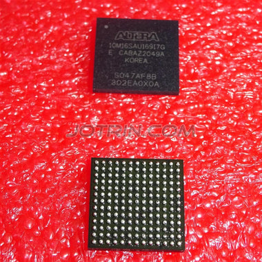
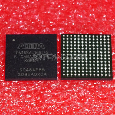
An FPGA is a "blank canvas" chip that can be reprogrammed after manufacturing. It contains a matrix of configurable logic blocks (CLBs) that engineers can rewire via software updates.
-
Flexibility: Can be updated to support new standards (like evolving 6G protocols) without replacing hardware.
-
Cost: Low upfront cost (no expensive mask sets), but higher unit cost and power consumption than ASICs.
-
Use Case: Prototyping new designs, Aerospace, Medical Imaging, Defense systems.
Comparison: ASIC vs. FPGA vs. SoC (2026)
| Feature | ASIC | FPGA | SoC |
|---|---|---|---|
| Reprogrammable? | No (Fixed hardware) | Yes (Field programmable) | Software only (CPU/NPU) |
| Performance | Highest (Optimized) | Moderate | High (Balanced) |
| Unit Cost | Low (at high volume) | High | Medium |
| Time to Market | Slow (18-24 months) | Fast (Instant) | Slow (12-18 months) |
4. Microprocessors & Microcontrollers
-
Microprocessor (MPU): The central "brain" (CPU) of a computer. It executes complex operating systems (Windows, Linux) but requires external memory and peripherals.
-
Microcontroller (MCU): A low-power, self-contained mini-computer used in embedded systems. It includes CPU, RAM, and Flash storage in one chip. Found in washing machines, car windows, and microwave ovens.
Ⅲ. The Chip Design Process: From Concept to Silicon
Designing a modern chip is a multi-year process involving massive teams and AI-powered Electronic Design Automation (EDA) tools. The cycle has evolved to include "Digital Twins" for verification before a single transistor is printed.

Step 1: Architecture & Specification
Engineers define the chip's "PPA" goals: Performance, Power, and Area. In 2026, this stage heavily involves deciding which IP blocks (Intellectual Property) to license, such as ARM cores for the CPU or specialized NPU designs for AI tasks.
Step 2: Logic Design (RTL)
Engineers write the code that describes what the chip does using Hardware Description Languages (HDL) like Verilog or VHDL. This code, known as RTL (Register Transfer Level), defines the logic gates and data flow.
Step 3: Functional Verification
Before physical design, the RTL code is tested using massive server farms. Verification ensures the logic is bug-free.
-
Formal Verification: Using mathematical algorithms to prove the logic is correct without running millions of test cycles.
-
Emulation: Running the design on specialized hardware (giant FPGAs) to simulate real-world speeds.
Step 4: Physical Design (Place & Route)
This is where the logical code is mapped to physical transistors. EDA tools place billions of components onto the virtual silicon canvas.
2026 Update: AI-driven tools now automatically optimize component placement to reduce wire length and heat generation, a task that used to take human engineers months.

Step 5: Tape-Out & Manufacturing
"Tape-out" is the final milestone where the GDSII file (the blueprint) is sent to the foundry (e.g., TSMC, Intel, Samsung). The foundry uses photolithography to print the circuit patterns onto silicon wafers using Extreme Ultraviolet (EUV) light.

Step 6: Packaging & Post-Silicon Validation
Once the wafer is sliced into individual dies, they are packaged.
Advanced Packaging (2.5D/3D): In 2026, chips are often stacked vertically or placed side-by-side (Chiplets) on an interposer to increase bandwidth. The final chips undergo rigorous electrical and thermal stress testing before shipping.