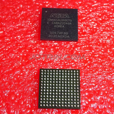
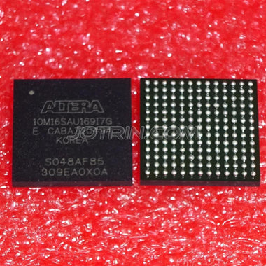
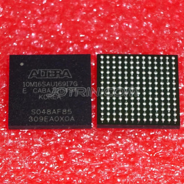
STM32F103C8T6 Datasheet, Pinout, Equivalents, and Specs
The STM32F103C8T6 is a mainstream 32-bit microcontroller unit (MCU) from STMicroelectronics, part of the STM32 F1 series. It integrates a high-performance ARM Cortex-M3 core operating at 72 MHz with 64 KB of Flash memory and 20 KB of SRAM. Its combination of processing power, extensive peripherals, and low-power modes has established it as a foundational component in industrial control, consumer electronics, and IoT applications.
What is the STM32F103C8T6?
The STM32F103C8T6 is a system-on-chip (SoC) microcontroller designed for embedded systems requiring a balance of performance, cost, and connectivity. Its internal architecture is based on the ARM Cortex-M3 core, which provides 32-bit performance with high code density thanks to the Thumb-2 instruction set. The device is engineered to deliver deterministic real-time behavior, making it suitable for control applications. It features a rich set of integrated peripherals, including multiple timers, communication interfaces (I2C, SPI, USART, USB, CAN), and analog-to-digital converters, which reduces the need for external components and simplifies system design. The target market spans from hobbyist development boards (e.g., the "Blue Pill") to high-volume commercial products in automation, metering, and peripheral device management.

STM32F103C8T6 Component Overview
Pinout Configuration and Packaging
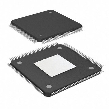
The STM32F103C8T6 is most commonly available in a 48-pin Low-profile Quad Flat Package (LQFP48). This package offers a good balance between pin density and ease of manufacturing. The pinout includes dedicated pins for power (VDD, VSS), analog inputs (VDDA, VSSA), clock sources (OSC_IN, OSC_OUT), and reset (NRST). The remaining pins are multiplexed to serve as General Purpose I/O (GPIO) or to connect to the internal peripherals. Critical pins for system setup include BOOT0 and BOOT1, which determine the memory space from which the device boots after a reset. For thermal management, the LQFP package relies on the PCB's copper planes for heat dissipation; a solid ground plane connected to the VSS pins is essential for stable operation under heavy processing loads.
Core Architectural Features
- ARM Cortex-M3 Core: The central processing unit is a 32-bit ARM Cortex-M3 core running at a maximum frequency of 72 MHz. It features a 3-stage pipeline and achieves 1.25 DMIPS/MHz, providing efficient execution for both control and data processing tasks.
- Memory Subsystem: The device contains 64 Kbytes of on-chip Flash memory for program storage and 20 Kbytes of high-speed static RAM (SRAM) for data. The memory architecture is designed for zero-wait state execution from Flash up to 24 MHz, with wait states required at higher CPU frequencies.
- Rich Peripheral Set: Connectivity is supported by a wide range of peripherals, including three USARTs, two SPI interfaces (18 Mbit/s), two I2C interfaces (400 kbit/s), a full-speed USB 2.0 device interface, and a CAN 2.0B controller. It also includes seven timers, including advanced control timers with PWM generation capabilities.
- Analog Interfaces: The MCU integrates two 12-bit Analog-to-Digital Converters (ADCs) with up to 10 channels, capable of 1 µs conversion times. This allows for direct interfacing with analog sensors without external ADC components.
Specifications Parameter Table
| Specification | Technical Details |
|---|---|
| Core Processor | ARM 32-bit Cortex-M3 |
| Maximum CPU Frequency | 72 MHz |
| Program Memory Size | 64 KB Flash |
| RAM Size | 20 KB SRAM |
| Operating Voltage (VDD) | 2.0V to 3.6V |
| I/O Ports (LQFP48) | 37 |
STM32F103C8T6 Equivalents, Cross Reference, and Lifecycle
The STM32F103C8T6 is an active component in mass production with a long-term availability outlook from STMicroelectronics. However, due to its high demand, supply chain constraints can lead to extended lead times. For purchasing managers and engineers facing allocation, several alternatives exist. The most notable is the GD32F103C8T6 from GigaDevice, which is widely recognized as a pin-to-pin compatible drop-in replacement. While the hardware footprint is identical, firmware migration may require recompilation with the GigaDevice software libraries and validation, as peripheral register behavior and clock timings can have minor differences. Another functional alternative, though not pin-compatible, is the AT32F403ACGU7 from Artery Tek, which offers similar performance and peripheral sets but requires a complete PCB redesign. Sourcing pin-to-pin replacements like the GD32F103C8T6 is a primary strategy for mitigating production delays without incurring hardware redesign costs.
Typical Application & Circuit Considerations
In system-level design, the STM32F103C8T6 is frequently used in motor control, industrial gateways, smart home devices, and USB peripherals. For reliable operation, proper power supply decoupling is critical. A 100nF ceramic capacitor should be placed as close as possible to each VDD/VSS pin pair to filter high-frequency noise. Additionally, a bulk capacitor (e.g., 4.7µF to 10µF) is recommended for the main power rail. When using an external high-speed crystal (HSE), the crystal and its two external loading capacitors must be placed very close to the OSC_IN and OSC_OUT pins with short traces to a local ground plane to ensure stable clock generation. The boot mode selection pins (BOOT0/BOOT1) must be configured with pull-up or pull-down resistors according to the desired boot source (e.g., on-chip Flash, system memory for bootloader, or SRAM).
Video Demonstration
Market Availability and Pricing Trends
As a high-volume, mainstream MCU, the STM32F103C8T6 is subject to market fluctuations in both pricing and lead times driven by global semiconductor supply and demand. Proactive sourcing and validation of compatible alternatives are key strategies for maintaining production continuity. To check real-time stock, pricing, or to request a quote for the STM32F103C8T6 and its verified alternatives, upload your BOM to WWDParts for fast processing.

Alan Carter
Senior Hardware Engineer & Component Specialist
Alan has over 15 years of expertise in embedded systems design, FPGA architecture, and global semiconductor supply chains. He specializes in component cross-referencing, lifecycle management, and helping OEMs navigate supply shortages.
Frequently Asked Questions (FAQs)
What is the current production lifecycle status and long-term availability of the STM32F103C8T6?
As of late 2023, the STM32F103C8T6 is in "Active" production status. STMicroelectronics includes this part in their 10-year longevity commitment program, which guarantees production for at least 10 years from its introduction. While it is a mature product, it is not scheduled for obsolescence and remains suitable for new designs, though newer families like the STM32G0 or STM32L series may offer better performance and power efficiency.
Are there any pin-compatible, drop-in replacements for the STM32F103C8T6 if it is out of stock?
The most direct pin-compatible upgrade within the ST family is the STM32F103CBT6, which is identical except for having 128KB of Flash memory instead of 64KB. Many third-party manufacturers, such as GigaDevice (GD32F103C8T6), produce pin-compatible clones. However, these clones may have subtle differences in peripheral behavior, electrical characteristics, and instruction timing, so thorough testing is required before using them as a production substitute.
What are the primary differences between the STM32F103C8T6 and the STM32F103CBT6?
The only significant difference is the on-chip Flash memory size. The 'C8' variant (STM32F103C8T6) has 64 Kbytes of Flash memory. The 'CB' variant (STM32F103CBT6) has 128 Kbytes of Flash memory. Both have 20 Kbytes of SRAM, operate up to 72 MHz, and are housed in the same LQFP48 package, making them pin-for-pin compatible. A project compiled for a C8 will run on a CB, but the reverse is only true if the code size is under 64KB.
What are the typical lead times for the STM32F103C8T6 from authorized distributors?
Lead times for the STM32F103C8T6 are highly volatile and depend on global supply chain conditions. During periods of high demand or shortages, factory lead times can extend from 30 to over 52 weeks. In a stable market, typical lead times might be closer to 12-20 weeks. It is crucial to check real-time inventory with multiple authorized distributors or work with a trusted independent distributor for more immediate stock availability.
What is the maximum reliable operating frequency, and what are the risks of overclocking?
The maximum guaranteed operating frequency for the STM32F103C8T6 is 72 MHz, achieved by using an external high-speed oscillator (HSE) with the internal PLL. While some individual units may function at higher frequencies (e.g., 84 MHz or more), this is outside the manufacturer's specification. Overclocking is not recommended for commercial products as it can lead to instability, unpredictable peripheral behavior, increased power consumption, and a significantly reduced operational lifespan due to thermal and electrical stress.
How many independent PWM channels are available on the STM32F103C8T6?
The STM32F103C8T6 features one advanced-control timer (TIM1) and three general-purpose timers (TIM2, TIM3, TIM4), all of which are 16-bit and have four independent channels each. This provides a total of 16 channels that can be configured for PWM output. TIM1 offers advanced features like complementary outputs with dead-time generation, which is ideal for motor control applications.
What are the risks associated with using low-cost "Blue Pill" boards or unmarked chips in a commercial product?
Many low-cost development boards and loose ICs sold online use remarked or clone chips (e.g., CS32, CKS32) instead of genuine STMicroelectronics parts. The risks of using these in a commercial product are significant: they may fail quality control, have different electrical characteristics, exhibit incorrect peripheral behavior (especially with ADC and USB), have a higher failure rate, and lack any form of traceability or warranty. For production, it is essential to source components from authorized distributors to guarantee authenticity.
What are the typical current consumption values in Run, Sleep, and Standby modes?
According to the datasheet, typical current consumption at 3.3V with all peripherals enabled is approximately 27 mA in Run mode at 72 MHz. In Sleep mode, with the CPU stopped but peripherals active, consumption drops to around 12 mA. In Standby mode (SRAM content retained, most clocks off), the current draw is very low, typically around 2 µA. These values are significantly higher than modern low-power MCUs like the STM32L series, making the F103 less suitable for battery-powered applications requiring long sleep intervals.
Looking for STM32F103C8T6 Inventory?
We offer competitive pricing, full traceability, and fast shipping for the STM32F103C8T6 and related components.
Check Stock & Request Quote